




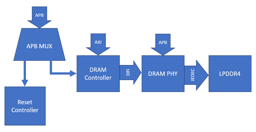
DRAM Controller integration in megaSoC
To enable full operating system support in megaSoC, a substantial amount of memory is required to accommodate the complexity of modern Linux-based software stacks, including the kernel, drivers, middleware, and user-space applications. Linux environments, unlike lightweight bare-metal systems such as nanoSoC, demand not only larger memory footprints but also consistent access to high-bandwidth memory to maintain performance across multitasking workloads. The most common approach is to incorporate external DRAM, which offers the necessary capacity and throughput. The use of DRAM enables the system to handle everything from file systems and networking to graphical interfaces and real-time data processing. Integrating a DRAM subsystem is a non-trivial challenge requiring the design and validation of a memory controller and physical interface (PHY) that can meet strict timing, signal integrity, and power constraints. A DRAM subsystem adds considerable complexity to the overall SoC design, both in terms of hardware implementation and system-level verification.
SoC Labs is very fortunate and thankful to Synopsys for providing access to their IP's for this project. They have supplied the Enhanced Universal DDR Memory Controller (uMCTL2) and their LPDDR4 multiPHY. Using these pre-verified IP's, should allow megaSoC to be a high-performance system with full OS support.
Specification
Before agreeing the appropriate IP with Synopsys a specification of the megaSoC system needs was developed. This enabled clear choses for the right IP for the project. The specifications included:
- Memory Type : LPDDR4
- This was chosen as we wanted megaSoC to emulate something like the Raspberry Pi or other single board computers.
- Speed: up to 2Gb/s
- We aren't targeting top-of-the-line computation, (otherwise we would probably go for LPDDR5). megaSoC needs enough bandwidth for reasonable applications to run.
- Bus Interface: AXI 4
After discussing with Synopsys, our requirements vs. their available IP, we came to the agreement of using the uMCTL2 and LPDDR4 multiPHY.
Configuration
The IPs have a significant number of configurable options, each of which adds complexity to the design and verification effort.
Integration
The design hierarchy is shown below. The top level wrapper includes a generate statement to allow for the inclusion of the Synopsys IP (or to not use it if users don't have access)
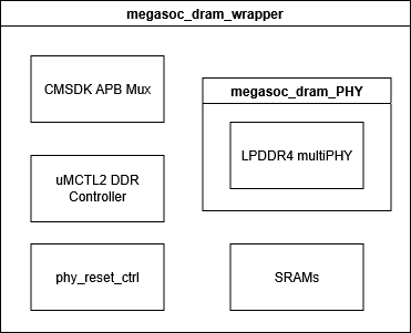
The main integration points are:
- Reset + clock control (including APB interface)
- APB interface on uMCTL2 and multiPHY
- AXI to uMCTL2
- SRAMs for PHY (this has a small CPU core to run the training algorithms)
- SRAMs for controller (buffers for write data)
- DFI interface between controller and PHY
- PHY to pins
- Interrupts
Other integration points that we are currently not focussing on:
- Scan interface to controller
- ATPG interface to PHY
- Bypass interface to PHY
All of these integration points need to be verified.
Verification
See the accordion below for all of the verification points
- Reset Controller
The reset controller is a small bit of custom IP to assert or de-assert the reset and power-ok pins
The address map for this is:
- 0x00 (bit 0) - ddrphy_reset
- 0x04 (bit 0) - ddrphy_pwrok
- 0x08 (bit 0) - ddrcore_rstn
This allows for independent control of all 3 signals. Further additions could be made to add things like clock enables for the IP
We need to verify the control of each of these 3 signals
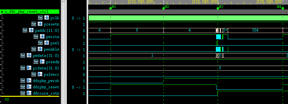
Looking at the above graph we can see
- after presetn - registers are default values (all zeros)
- At M1 - write to 0x00 sets ddrphy_reset high
- At M2 - write to 0x04 sets ddrphy_pwrok high
- Before M3 write to 0x00 to set ddrphy_reset low
- At M3 - write to 0x08 to set ddrcore_rstn high
- At M4 write to 0x04 to set ddrphy_reset high
As a very simple IP, this shows the working principle.
- APB interface on uMCTL2 and multiPHY
APB read and write to the controller and PHY is needed to control their behaviour
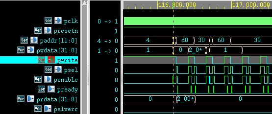
This one is fairly straightforward. We added an APB interface to the main system bus of megaSoC and can run read and write commands to the PHY and controller successfully
TO NOTE - the PHY data/address alignment was not to 32 bits. We had to shift the addressing by 2 so that the system bus / CPU could properly access the registers for 32 bit word aligned accesses
- SRAMs for PHY
The SRAMs for the PHY are used to program the PHY training routines. There is an instruction memory and data memory
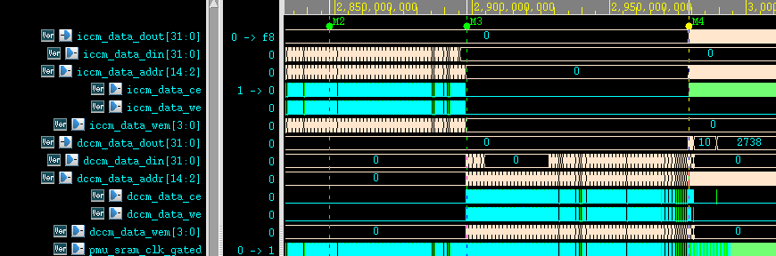
Looking at the above waveforms you can see
- M2 - programming iccm (instruction memory)
- M3 - programming dccm (data memory)
- M4 - boot started for the PHY training. Reading from iccm and dccm
Whilst this does not fully verify the behaviour of the SRAMs. This shows that they can be programmed and read from by the PHY to run the training program.
- SRAMs for controller
Currently, we would only be able to observe this behaviour once the subsystem is running AXI write transactions and we have not yet got that working. For now this is on hold.
- DFI interface between controller and PHY
Our first approach at this was to test this using AXI based transactions. This would mean that the DFI interface is tested functionally. However, getting it to the point of running AXI transactions is currently not working. We suspect that this is in the configuration of the PHY init training software but we can't be fully sure that it is not a problem in the DFI interface.
The slight complexity here is that the controller has a single DFI interface, but the PHY breaks it up into phases, so you have to select which bits from the controller correspond to the correct phases in the PHY. These phases are needed because of the ratio in clocks between the phy and controller (typically either 1:1, 2:1, or 4:1)
What we are currently trying to do is add a monitor that sits between the controller and PHY to ensure correctness of the connections. This monitor comes from the VC - VIP portfolio from Synopsys, we can add a UVM component to monitor signals here.
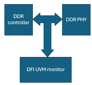
The idea is shown above, but currently this is not finished work
- PHY to pins
Check connection from PHY to pinout in testbench. This will be verified by checking that the target device in the testbench is recieving values from the DDR multiPHY.
- AXI to uMCTL2
After training and initialisation is complete, we should be able issue AXI requests to read and write to the DRAM.
- Interrupts
Not yet decided how to test these
Update on PHY verification (12/05/26)
After discussing with synopsys, one issue they raised is that maybe the problem with the PHY interacting with the device in the testbench is that the device is not setup correctly. I was using the synopsys VIP for the LPDDR4 device and what we could see from the simulation environment was as below
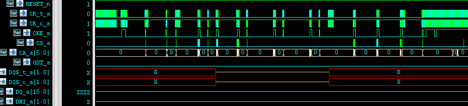
With this we can see that the PHY sets the DQS pins to Z's, this looks like the PHY is expecting some response from the device but isn't recieving it. We can also see some activity happening on the CA pins that look like it's trying to initialise the device.
If we replace the Synopsys VIP with an LPDDR4 model from micron we instead see this:
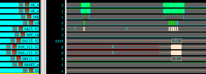
This is much more of what we expect. Unfortunately the model from micron is really designed to be tested at full speed (i.e. timing must be adhered to for pulse widths etc.) This also doesn't work to completion as the log shows below:
PU-CAL = VDDQ/3 @ FSP_WR = L
PPRP mode disable.
PDDS = RZQ/1 @ FSP_WR = L
Fast response (high current) mode (VRCG = H)
Frequency set point[0]
Normal operation (MR13 OP2 = L)
PU-CAL = VDDQ/3 @ FSP_WR = H
PPRP mode disable.
PDDS = RZQ/1 @ FSP_WR = H
DQ_ODT = RZQ/3 @ FSP_WR = H
CA_ODT = RZQ/3 @ FSP_WR = H
 Vref_CA_Range = 1'b1 and Vref_CA = 6'b001101  set @ FSP_WR = H
 Vref_DQ_Range = 1'b0 and Vref_DQ = 6'b101011  set @ FSP_WR = H
SoC_ODT Disable @ FSP_WR = H
ODT-CK  = 1'b1
ODT-CS  = 1'b1
ODT-CA  = 1'b0
PPRE mode disable.
No offset, 5 C gradient ( MR4_OP[6:5] ).
TRR mode disable
Fast response (high current) mode (VRCG = H)
Frequency set point[1]
Normal operation (MR13 OP2 = L)
Error: megasoc_tb.g_ddr_model.u_lpddr4_dram1.ins_1ch.PROTECTED 4169238 ns   MRW_2 command is illegal input.
Normal operation (VRCG = L)
Frequency set point[1]
Normal operation (MR13 OP2 = L)
Error: megasoc_tb.g_ddr_model.u_lpddr4_dram1.ins_1ch.PROTECTED.task_lpddr4_MRW_2_command_check 4174252 ns  MRW_2 command need to input consecutively after MRW_1 command input.
Whilst using this model will be very useful to check the final functionality of the DDR controller and PHY, the simulation times will take too long whilst development is ongoing. The good news from this is that we think the PHY is starting to work correct but have identified a problem in the model. Next steps are to try and fix the VIP setup so that this will work correctly.
Rethinking the Verification Methodology (16/09/2025)
Given the number of simulations needed to run to validate the integration of this IP, we decided to try and speed up the simulation approach as much as possible. One way to do this was to stop simulating it within the megaSoC environment and create a smaller subsystem to validate the IP in isolation. This removes significant simulation time used to boot the Cortex A53 and other IP's that aren't really needed for this first step in the validation
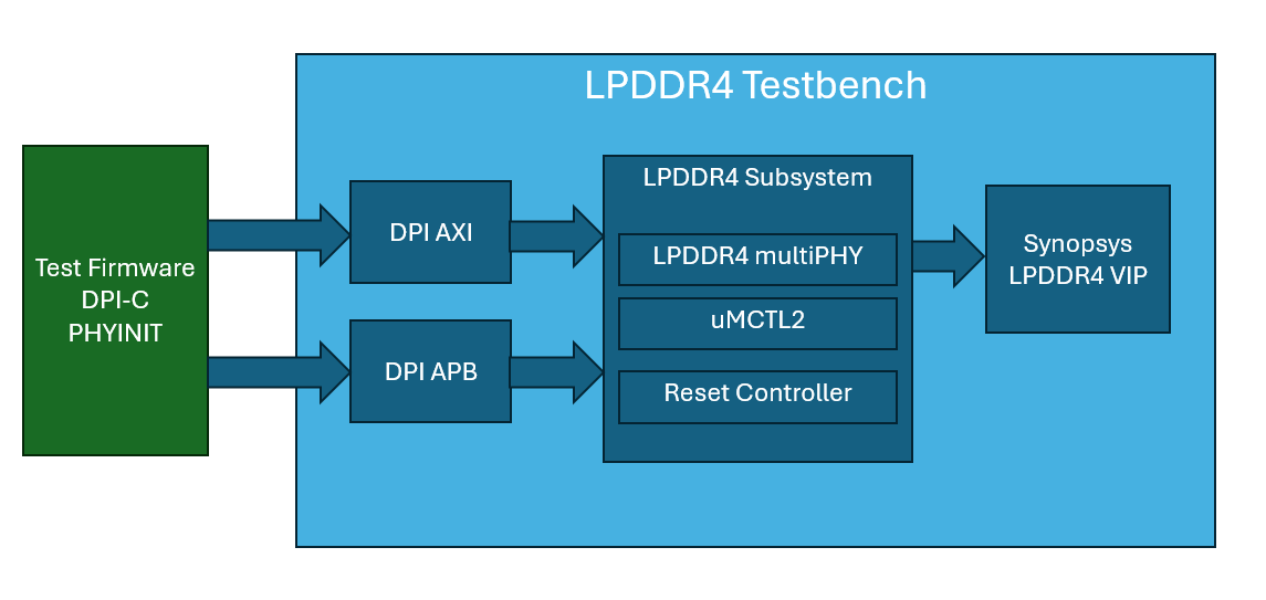
A simplified subsystem was created using a UVM testbench and DPI-C components so that the PHY test firmware and PHY initialisation firmware can be run directly in the simulator. This test bench includes the Synopsys LPDDR4 VIP. This was instantiated and configured based on the tb_lpddr4_svt_verilog_basic_sys example that Synopsys provide with their VC-VIP package.
Using this method has significantly reduced simulation and compile time for validating this IP. Currently the status is that the PHY will run PHYINIT, we do still get a few UVM errors from the VIP model but this is very good progress in the right direction. What we currently see as output from the simulation is:
Final LPDDR memory Configuraton: DRAM Tests
** Start DDR CTRL Init **
SWSTAT.B.sw_done_ack != 0
** Start DDR PHY Init **
Reset PHY
** STEP E **
Set clock to Pstate 0
UVM_INFO /eda/synopsys/2022-23/RHELx86/VC-VIP-SOC_2022.12/vip/svt/lpddr_svt/U-2022.12/sverilog/src/vcs/svt_lpddr4_jedec_fsm.svp(1624) @ 285085159800: lpddr4_tb_memory_memory_LPDDR_AGENT [Initialization] Initialization completed for LPDDR4
APBONLY.UctWriteOnlyShadow: 0x00000000
Wrote 0 to ABPONLY.DctWriteProt
Wrote 1 to ABPONLY.DctWriteProt
Mail = 0x00000000
UVM_WARNING /eda/synopsys/2022-23/RHELx86/VC-VIP-SOC_2022.12/vip/svt/common/T-2022.09/sverilog/src/vcs/svt_err_check_stats.svp(583) @ 527819544800: lpddr4_tb_memory_memory_LPDDR_AGENT [register_fail:initialization_group:LPDDR4:tckb_during_initialization_for_mrw_mrr_cmd_check] Description: During the initialization when MRW/MRR command is issued, clock period shall be within the defined range of tCKb (18ns to 100ns), Reference: LPDDR4C JEDEC Spec:3.3 Power-Up, Initialization & Power-Off Procedure / Initialization Timing Parameters - During Initialization MRW should be performed at boot clock within time period[18.000000ns, 100.000000ns], Actual clock period =1.248000ns
UVM_WARNING /eda/synopsys/2022-23/RHELx86/VC-VIP-SOC_2022.12/vip/svt/common/T-2022.09/sverilog/src/vcs/svt_mem_core.svp(658) @ 549417048800: lpddr4_tb_memory_memory_LPDDR_AGENT.mem_sequencer [SNPS/SVT/MEM/CORE/RD_B4_WR] Address: 0x0000000000000000 a location was read before it was initialized or written
UVM_WARNING /eda/synopsys/2022-23/RHELx86/VC-VIP-SOC_2022.12/vip/svt/common/T-2022.09/sverilog/src/vcs/svt_mem_core.svp(658) @ 549417048800: lpddr4_tb_memory_memory_LPDDR_AGENT.mem_sequencer [SNPS/SVT/MEM/CORE/RD_B4_WR] Address: 0x0000000000000001 a location was read before it was initialized or written
UVM_WARNING /eda/synopsys/2022-23/RHELx86/VC-VIP-SOC_2022.12/vip/svt/common/T-2022.09/sverilog/src/vcs/svt_mem_core.svp(658) @ 549417048800: lpddr4_tb_memory_memory_LPDDR_AGENT.mem_sequencer [SNPS/SVT/MEM/CORE/RD_B4_WR] Address: 0x0000000000000002 a location was read before it was initialized or written
...
We see a lot of these UVM_WARNING around reading from uninitialized space (which according to the PHY documentation is absolutely fine to ignore), after a lot of the same messages the rest of the firmware continues:
APBONLY.UctWriteOnlyShadow: 0x00000002
Wrote 0 to ABPONLY.DctWriteProt
Wrote 1 to ABPONLY.DctWriteProt
Mail = 0x00000002
APBONLY.UctWriteOnlyShadow: 0x00000001
Wrote 0 to ABPONLY.DctWriteProt
Wrote 1 to ABPONLY.DctWriteProt
Mail = 0x00000001
APBONLY.UctWriteOnlyShadow: 0x000000fe
Wrote 0 to ABPONLY.DctWriteProt
Wrote 1 to ABPONLY.DctWriteProt
Mail = 0x000000fe
APBONLY.UctWriteOnlyShadow: 0x00000007
Wrote 0 to ABPONLY.DctWriteProt
Wrote 1 to ABPONLY.DctWriteProt
Mail = 0x00000007
** TRAINING SUCCESSFUL **
** Finish DDR PHY Init **
Wrote 0 to SWCTL.B.sw_done
SWSTAT.B.sw_done_ack != 0
Wrote 1 to DFIMISC.B.dfi_init_start
Wrote 1 to SWCTL.B.sw_done
SWSTAT.B.sw_done_ack != 0
Warning!! Icco =    2mA, is too high, vp is the vref of vreg_v2i @ time = 924839 ns!
DFISTAT.B.dfi_init_complete != 0
Wrote 0 to SWCTL.B.sw_done
Wrote 0 to DFIMISC.B.dfi_init_start
Wrote 1 to DFIMISC.B.dfi_init_complete_en
Wrote 0 to PWRCTL.B.selfref_sw
Wrote 1 to SWCTL.B.sw_done
SWSTAT.B.sw_done_ack != 0
UVM_ERROR /eda/synopsys/2022-23/RHELx86/VC-VIP-SOC_2022.12/vip/svt/common/T-2022.09/sverilog/src/vcs/svt_err_check_stats.svp(583) @ 1146227023800: lpddr4_tb_memory_memory_LPDDR_AGENT [register_fail:fsm_group:LPDDR4:invalid_command_during_self_refresh_state_check] Description: During Self Refresh mode SDRAM can accept the following commands, MRR-1, CAS-2, SRX, MPC, MRW-1, and MRW-2 except PASR Bank/Segment setting, Reference: LPDDR4C JEDEC Spec:4.21 Self Refresh Operation - Received command = REFRESH_ALL_BANK
STAT.B.operating_mode != 0
=== AXI Write/Read Test ===
AXI write 0xA5A5A5A5A5A5A5A5 to 0x00008000
From the Mail-box from the PHY processor we see in order 0x0, 0x2, 0x1, 0xFE and 0x07 which relates to the phases of the training as it completes with 0x07 signaling the successful completion of the initialisation.
Once control is handed over to the uMCTL2 controller we see the UVM error relating to an invalid command. One thing to note is that the PHY documentation suggests disabling some of the refresh errors as these don't seem to run in the simulation environment (or at least when the simulation speed-ups are enabled), we may actually just be able to disable this error at this level of system verification.
This seems to complete the phy-initialization validation, however currently the DPI-AXI component needs some work to fix, as currently an AXI transaction is never seen by the controller.
Update 01/10/26
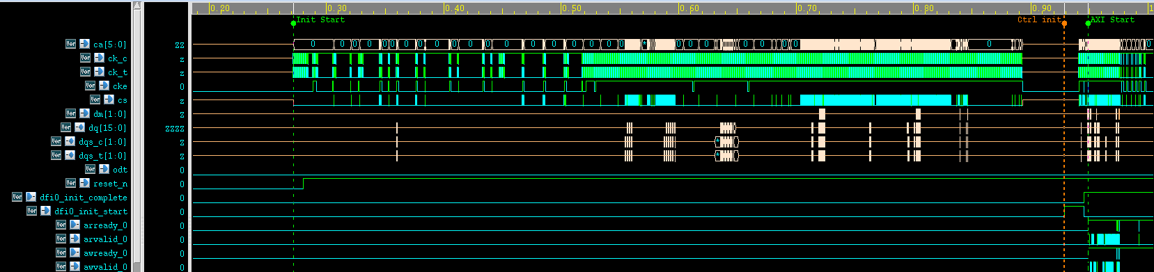
We finally see working behaviour in the LPDDR4 subsystem. The bug was in the software/register configuration of the controller side, which had not been completed, as well as some mismatches in the write-data buffer interface, so it never properly went into mission mode. With these fixed, the AXI interface properly passes transactions to the DRAM controller, which successfully communicates to the LPDDR device in the testbench. Currently Shiva has implemented a number of verification testcases as shown below:
| Test | Result |
|---|---|
| 256-beat burst, data path | 256/256 beats |
| Address-map walk: every address bit, all banks, top row, end of 256 MB | no aliasing |
| Byte-strobed writes, merges, neighbour integrity (read-modify-write path) | pass |
| Concurrent traffic: bank interleave, row thrash, read/write mix | pass | | pass |
| Refresh, automatic and software self-refresh, data retained | pass |
Constrained-random traffic vs a C shadow model (DRAM_SEED=<n>) | 10 seeds, 0 mismatches |
| Narrow 8/16/32-bit transfers at every aligned offset | all pass |
As you can see from the below waveform, the PHY starts initialisation, the controller initialises and then we have interrogation of the DRAM device from the AXI-ctrl-PHY path. While this shows implicitly that the subsystem is working, we have not yet exhausted the list of verification points that are needed to say this is fully verified.
Project Milestones
Do you want to view information on how to complete the work stage ""
or update the work stage for this project?
-
IP Selection
Design FlowTarget DateCompleted DateResult of WorkAfter discussing with synopsys the IP needs, they have suggested the uMCTL2 and LPDDR4 multiPHY
-
Getting Started
Design FlowTarget DateCompleted DateResult of WorkThe scope of this project is to integrate the DDR controller and PHY. Verify the functionality. Run synthesis on the design before integrating into the hierarchical design flow for the full megaSoC
-
Specifying a SoC
Design FlowTarget DateCompleted DateResult of WorkmegaSoC is the target for this work
-
Verification Methodology
Design FlowTarget DateCompleted DateResult of WorkWe'll be using a mixture of UVM based components from the Synopsys VC-VIP suite, and functional verification by passing vectors from the Cortex A53 to the memory model in the testbench
-
Architectural Design
Design FlowTarget DateCompleted DateResult of WorkArchitecture of the subsystem complete
-
Generate RTL
Design FlowTarget DateCompleted DateResult of WorkGlue logic for the subsystem is complete. As well as design of a reset controller for local reset behaviour
-
RTL Verification
Design FlowTarget DateVerify the functional behaviour of the controller and PHY working together
-
Simulation
Design FlowCompleted DateSimulation environment setup and working
Team




 Project Creator
 Daniel Newbrook
Digital Design Engineer
at University of Southampton
Research area: IoT Devices
ORCID Profile
 Hardware design
Submitted on
Comments
Configuration
We are very terse with the statement on configuration. Can we share any further detail?
Can we state any actual numbers for simulation and compile time?
"Using this method has significantly reduced simulation and compile time for validating this IP." I can't see any place we discuss how long these runs were taking and are now taking. Of course this is dependent on the compute resources assigned but I think giving some view of how long such runs take would be helpful.
SRAMs
In the early write up it is said:
The recent write up says the AXI transaction are now working but I can't see an update on this SRAM activity.
Today's Team review
I note the point made "we have not yet exhausted the list of verification points that are needed to say this is fully verified". At today's SoC Labs team review Shiva said he was still working on the DRAM test cases. It would be great if we could add a bit more detail on the status of the work in terms of the expected remaining list of verification points and expected effort.
John.
Sorry for the confusion. As…
Sorry for the confusion. As described in the Update 01/10/26, the standalone LPDDR4 subsystem is verified against its planned standalone test list (T1–T8). It is now integrated into MegaSoC as a submodule. It is wired in behind a build option (
INC_LPDDR4), with an AXI async bridge, an AHB→APB async bridge, and plumbing from the chip down to the testbench. Both builds compile clean, and as of today the A53 firmware brings up the DRAM and the first read/write tests (T1–T3) pass inside MegaSoC.Interest in Collaboration
Hi everyone! I’m interested in collaborating on projects within the SoC Lab.
My primary areas of interest are Design Verification (DV), Formal Verification, and AI for hardware design and verification.
I’d be happy to connect with the team and contribute for the project.
Thanks!
Nikhitha
Add new comment
To post a comment on this article, please log in to your account. New users can create an account.