SDIO Controller Verification
Project Overview
SoC Labs reference designs, such as megaSoC, are developed to allow integration of open source IP along with the core Arm AAA licensed IP to create complete System on Chip implementation.
This projects aim is to integrate of an open source SD Card interface submodule into megaSoC with a focus on developing a clear verification strategy to ensure it is know to work, end-to-end, to provide a persistent storage mechanism.
Modern embedded SoCs usually require some persistent storage to store configuration, log data, and exchange files. The industry standard SD Card is an ideal medium for this. MegaSoC can integrate open source IP to support SD Card. This project uses the open source ZipCPU sdspi controller as the basis for a SD card interface submodule of MegaSoC that supports SPI, SDIO, and eMMC modes from a single RTL codebase.
The SD Card standards supports a variety bus interface and data transfer performance needs. This project targets the SDIO 4-bit native mode path, using the sdiodrv.c driver.
Integrating a new submodule and knowing it works end-to-end are two very different things. In this case, a controller that synthesises cleanly and passes unit-level RTL simulation can still stall indefinitely during card initialisation, produce silent data corruption on block boundaries, or behave differently across the many and varied SD card brands. A goal of this project is to develop a layered verification strategy to look to address these end to end system challenges. The motivation is partly motivational, any MegaSoC application that depends on persistent storage needs a trustworthy foundation and partly practical as the sdspi controller has a known latent issue in its sdrxframe receive module, identified through formal verification, that simulation alone may never have exposed.
The first stage in the layered verification strategy is confirming the correct raw block read and write behaviour at the driver level through C-based integration tests, then building upward to verify the filesystem operations over the same hardware path.
Software-to-Hardware flow
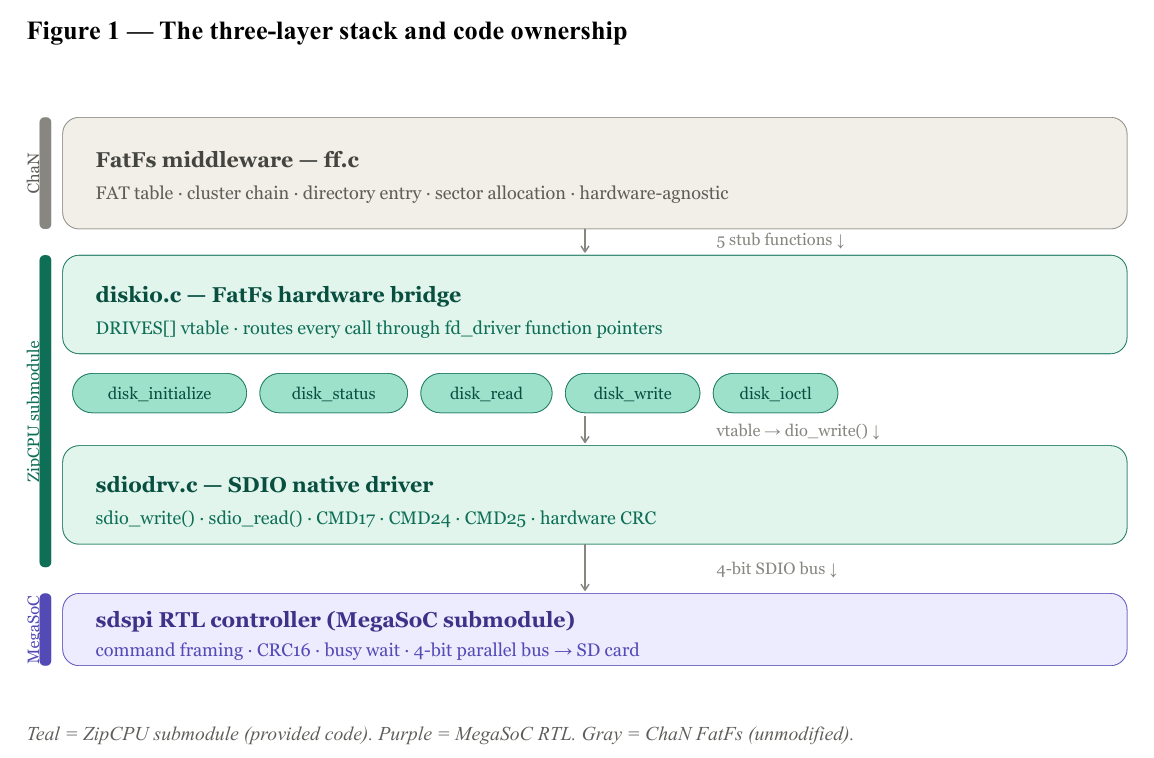
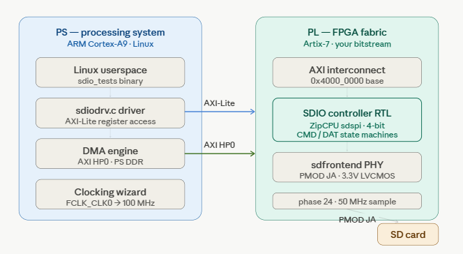
Writing a file through the full software stack involves three layers, each provided by a different source and each with a clearly defined responsibility. Understanding exactly how they connect — and where the boundaries are — is both the intellectual contribution of this integration work and the foundation of the verification methodology.
To implement the top level file system support, FatFs, the open-source filesystem middleware by ChaN, has been chosen as it fits with the SoC Labs ethos of minimising system resource use, and therefore cost, as this implementation has been used in many microcontrollers and embedded systems as it takes up little space in memory.
FatFS handles all filesystem-level concerns: FAT table maintenance, cluster chain resolution, directory entry management, and sector allocation. FatFs is deliberately hardware-agnostic. It communicates downward through exactly five stub functions — disk_initialize, disk_status, disk_read, disk_write, and disk_ioctl — which it calls without any knowledge of what lies beneath them.
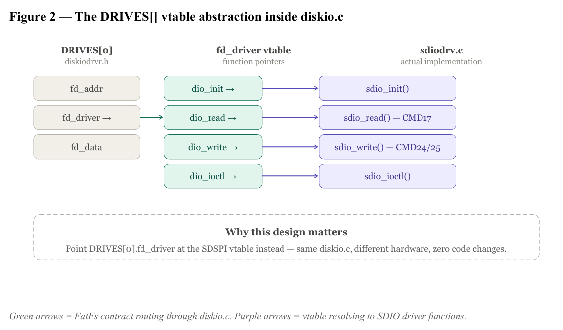
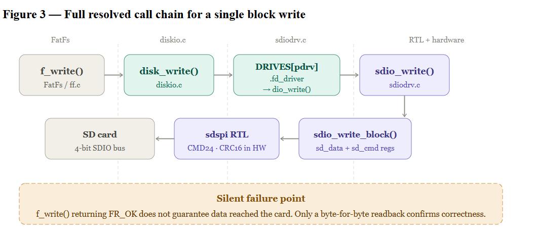
Those five stubs are implemented in diskio.c, which is provided as part of the ZipCPU sdspi submodule rather than written from scratch. What makes this implementation architecturally interesting is that it does not call the SDIO driver directly. Instead, every stub routes through a driver abstraction table — DRIVES[], defined in diskiodrvr.h — where each entry holds a hardware base address (fd_addr), a vtable of function pointers (fd_driver: dio_init, dio_read, dio_write, dio_ioctl), and a live driver handle (fd_data) populated at initialisation time. A disk_write() call therefore resolves through the chain: DRIVES[pdrv].fd_driver->dio_write(DRIVES[pdrv].fd_data, sector, count, buff). The SDIO driver is plugged into this table at startup — meaning the same diskio.c can serve either the SDSPI or SDIO backend without modification, simply by changing the table entry. This is a clean separation of concerns. This separation of concerns was not only determined but was also verified as part of this project, not assumed.
The bottom layer is sdiodrv.c, part of the SD Card submodule, which the DRIVES[] vtable points to at runtime. It translates dio_read and dio_write calls into native SDIO commands over the 4-bit parallel bus: CMD17 for single block reads, CMD24 for single block writes, CMD25 for multi-block writes. CRC generation and checking is handled entirely in hardware by the sdspi RTL controller. The addressing mode — byte for SDSC, block for SDHC/SDXC — is determined once during sdio_init() from the CCS bit in the ACMD41 response and applied automatically to every subsequent transfer.
There is one detail the layer description alone does not make visible: disk_initialize calls dio_init, which calls sdio_init(), which executes the full SDIO initialisation sequence. FatFs triggers this once, at f_mount() time, and trusts the result completely. If sdio_init() returns NULL, disk_initialize returns STA_NODISK, FatFs returns FR_NOT_READY, and nothing in that chain tells you which step of initialisation failed. This opacity is precisely why the initialisation sequence is tested and documented independently before FatFs is involved — the integration test results in this project provide the evidence that the full sequence completes correctly in simulation, confirmed by PASS: sdio_init returned a valid driver handle in the test output.
SDIO Initialisation:
Fully understanding the initialisation sequence matters for integration testing because each stage introduces a new failure mode that C test code needs to handle correctly. The sequence is orchestrated entirely by sdio_init(), and it does far more than simply wake the card up — it negotiates the operating voltage, identifies the card, assigns it an address on the bus, selects it, widens the bus from 1-bit to 4-bit, and then attempts to step the clock up through a hierarchy of high-speed modes depending on what both the card and the PHY can support. If any stage fails, the driver has explicit error paths that either bail entirely or degrade gracefully to a slower mode. The acknowledged limitations stated are the driver currently handles only 3.3V mode even if 1.8V switching hardware exists, and it does not recover well from a failed initialisation.
| Command / Action | Driver Function | Register Value | Response Expected | What to Check | Failure Mode / Notes |
|---|---|---|---|---|---|
Controller reset + PHY setup | sdio_init() | sd_cmd = SDIO_RESET | SDIO_REMOVEDsd_phy = SPEED_SLOW | SECTOR_512B | Poll SDIO_HWRESET until clear | Clock confirmed at 400 kHz. Poll until SPEED_SLOW reflected back in PHY register. | [PHY phase] Clock phase set based on frontend type: SERDES→20, DDR/raw→16. Wrong phase causes marginal data capture — CMD19 tuning later corrects this. |
CMD0 — GO_IDLE_STATE | sdio_go_idle() | sd_data = 0sd_cmd = SDIO_REMOVED | SDIO_CMD | SDIO_RNONE | SDIO_ERR | None | No response byte to decode. Simply wait for busy to clear. Card enters idle state. | Check for timeout conditions while waiting. |
CMD8 — SEND_IF_COND | sdio_send_if_cond() | sd_data = 0x01a5 (VHS=1, pattern=0xA5)sd_cmd = SDIO_READREG + 8VHS=1 -> voltage rage 2.7 - 3.6V | R7 via SDIO_READREG — lower byte echoes pattern (0x01a5) | Check lower byte of response = 0xA5. If 8 != (hcs & 0x80ff) → card is not high capacity capable → hcs=0. | [Critical branch] If echo ≠ 0xA5 → driver frees memory and returns NULL, No retry. If no response → assume non-HCS, continue with hcs=0. |
ACMD41 — query (opcond=0) | sdio_send_op_cond() | sd_data = op_cond_query (initially 0)sd_cmd = SDIO_READREG + 41 | R3 — OCR register. Stored in dev->d_OCR | Mask response with 0x0ff8000 to extract voltage ranges. If result = 0, no compatible voltages → bail. | [Voltage probe] First ACMD41 is a query with opcond=0. If SDPHY_1P8VSPT set in PHY, driver adds S18R | XPC flags to next call. |
ACMD41 — poll loop | sdio_send_op_cond() | sd_data = op_cond_query (includes HCS/S18R/XPC flags after initial probe) | R3 (OCR) with bit 31 = 1 indicates card power-up complete; loop exits when set | Poll OCR[31] until set (card ready). Verify CCS (bit 30) captured in dev->d_OCR for addressing mode selection. | [No timeout — Critical] Poll loop has no timeout guard. A card that never raises bit 31 hangs forever. Wrap sdio_init() with an external watchdog in your test code. |
CMD11 — VOLTAGE_SWITCH (conditional) | sdio_send_voltage_switch() | sd_cmd = (SDIO_ERR | SDIO_READREG) + 11 | R1 — check SDIO_ERR bit | Only executed if SDPHY_1P8VSPT set AND d_OCR has CCS and S18R. | [Known limitation] This controller only handles 3.3V mode. Even if hardware exists for switching to 1.8V, this driver doesn't (yet) enable it. The controller doesn't really recover well from a failed init. |
CMD2 — ALL_SEND_CID | sdio_all_send_cid() | sd_cmd = (SDIO_ERR | SDIO_READR2) + 2 | R2 (136-bit) — 4×32-bit words from sd_fifa into d_CID[] | CID contains manufacturer ID, product name, serial number, manufacture date. Logged via sdio_dump_cid() if SDINFO=1. | [SDIO only] Does not exist in SPI mode. Useful during bring-up to confirm correct card identity. |
CMD3 — SEND_RELATIVE_ADDR | sdio_send_rca() | sd_cmd = (SDIO_ERR | SDIO_READREG) + 3 | R6 — upper 16 bits = RCA. Stored as dev->d_RCA = (r >> 16) & 0xffff | RCA used by every subsequent targeted command. If CMD3 errors, driver retries once before returning RCA=0. | [Silent failure risk] If both CMD3 attempts fail, RCA=0 is returned silently. CMD7 then selects no card. All subsequent reads/writes time out with no clear error. |
| CMD10 SEND_CID3.3V path — called before CMD7 | sdio_send_cid() | sd_data = d_RCA << 16 sd_cmd = (SDIO_ERR | SDIO_READR2) + 10 | R2 (136-bit) — 4×32-bit words from sd_fifa into d_CID[] | Reads manufacturer ID, product name, serial number, manufacture date using the RCA assigned by CMD3. Card must be in Stand-by state (not yet selected by CMD7) | In the 3.3V path, CMD10 is called before CMD7 because the card is still in Stand-by state and accepts CID read commands. In the 1.8V path this is reversed — card must be temporarily unselected because cannot execute either CMD10 or CMD9 from the transfer state. |
| CMD9 SEND_CSD - called before CMD7 | sdio_read_csd() | sd_data = d_RCA << 16 sd_cmd = (SDIO_CMD | SDIO_R2 | SDIO_ERR) + 9 | R2 (136-bit) — 16 bytes of CSD register read via sd_fifa into d_CSD[] | Driver decodes CSD_STRUCTURE (bits [127:126]) to choose parsing path. CSD_STRUCTURE=1 (SDHC) → d_sector_count = (C_SIZE+1) * 1024. CSD_STRUCTURE=0 (SDSC) → more complex calculation | [Silent failure risk] d_sector_count and d_block_size are only populated here they are 0 until CMD9 completes. . If CMD9 fails silently or returns invalid data, disk_ioctl(GET_SECTOR_COUNT) returns 0, and FatFs refuses to mount. |
CMD7 — SELECT_CARD | sdio_select_card() | sd_data = d_RCA << 16sd_cmd = (SDIO_ERR | SDIO_READREGb) + 7 | R1b — card transitions Stand-by → Transfer state | Without CMD7, all data commands (CMD17, CMD24) are ignored. Uses R1b to handle card-busy phase after selection. | [Critical] If RCA from CMD3 was 0 (silent failure), CMD7 selects no card. All subsequent operations time out with no diagnostic distinguishing this from other failures. |
| ACMD51 - SEND_SCR | sdio_read_scr() | sd_phy sector = SECTOR_64B (3<<24) sd_cmd = (SDIO_ERR | SDIO_MEM | SDIO_READREG) + 51 Preceded by CMD55 via sdio_send_app_cmd() | 64-bit SCR register — 2×32-bit words from sd_fifa into d_SCR[8] | Key bits in SCR[1]: bit 2 = 4-bit bus support. If set → ACMD6 issued next and SDPHY_W4 enabled. If clear → bus stays 1-bit.line 2220: if (dv->d_SCR[1] & 0x04 | [Bus width gate] SCR is the sole decision point for 4-bit bus width in the 3.3V path. On real PYNQ-Z2 hardware with a real SD card, this bit will be 1, enabling ACMD6 and 4× throughput improvement. Verifying this transition is a concrete hardware-vs-simulation difference to document. |
ACMD6 — SET_BUS_WIDTH | sdio_set_bus_width(dv,2) | sd_data = 2 (4-bit)sd_cmd = SDIO_READREG + 6sd_phy |= SDPHY_W4 | R1 — check no error bits set | Widens bus from 1-bit to 4-bit. PHY and card must both be updated — mismatch causes all data transfers to fail. | [1.8V path only] ACMD6 currently only called in 1.8V PHY path. At default 3.3V, bus stays 1-bit — limits throughput by 4×. L |
CMD6 — SWITCH_FUNCSpeed negotiation | sdio_switch() | Query: 0x00fffff3Switch: 0x80fffff1–4 (mode dependent) | R1 + 512-bit status block via sd_fifa | Driver probes SDR104→DDR50→SDR50→SDR25 in order. Falls back to SDR12 if none succeed or PHY cannot sustain speed. | [Speed hierarchy] SDR104 (200 MHz) → DDR50 → SDR50 → SDR25 → SDR12 (25 MHz default). Each checked against PHY before card switch committed. Lines 1977–2150. |
| Init complete | sdio_init() returns SDIODRV *dv | sd_phy reflects final negotiated speed + bus width | Non-NULL = success. NULL = fatal failure (memory, voltage mismatch, or CMD8 echo fail). | Addressing mode determined by dev->d_OCR & 0x40000000 (CCS bit). Used in every subsequent read/write call. |
Verification Strategy:
This project addresses verification at two distinct levels: functional correctness of the SDIO controller integration through C-based testing in simulation, and physical correctness through hardware validation on a PYNQ-Z2 FPGA platform. The downstream design flow — from gate-level netlist through to ASIC implementation — is handled within the main MegaSoC project and is out of scope here.
The verification approach is intentionally layered. Simulation establishes that the software stack and RTL controller interact correctly under ideal conditions. Hardware validation then confirms that the same integration survives contact with a real SD card, a real AXI bus, and real signal timing — conditions that behavioural simulation cannot reproduce. Simulation without hardware leaves timing and card variability unverified, while hardware bring-up without prior simulation makes debugging exponentially harder because software bugs and hardware bugs become indistinguishable.
C-based Integration Testing in Simulation
Functional correctness is established through a structured C test suite (sdio_tests.c) compiled against the MegaSoC software stack and executed against the RTL simulation. The test suite exercises fourteen scenarios covering initialisation, card information validity, single block read, read repeatability, single block write with readback, multi-block write with readback, invalid argument handling, a repeated transfer stress test across eight iterations and corner cases verification as well . Pass criteria are explicit for each test: sdio_init() must return a non-NULL handle, card parameters (OCR, RCA, block size, sector count) must be non-zero and self-consistent, and every write/readback comparison must match byte-for-byte using compare_buffers().
The simulation model (mdl_sdio.v) was itself modified during this project to correctly respond to ACMD51 (SCR register transfer), CMD6 (SWITCH_FUNC status block), and the CMD24/CMD25 write path with DAT0 busy indication. This is an important limitation to state explicitly: the simulation model was modified while executing the tests. This is not a weakness of the testing methodology — it is a known and documented constraint that motivates the hardware validation phase.
All fourteen test cases currently pass in simulation with zero errors, confirmed by the ** TEST PASSED ** output and Total SDIO errors = 0. The simulation log provides timestamped evidence of each command transaction — CMD17 and CMD24 sector addresses, data patterns at write and read, and CRC results — making the result reproducible and auditable.
Hardware Validation on PYNQ-Z2
For full integration confidence, the design will be validated on a physical PYNQ-Z2 development board connected to a real microSD card. The PYNQ-Z2 carries a Xilinx Zynq-7000 SoC (XC7Z020), which combines Artix-7 FPGA fabric with a hard dual-core ARM Cortex-A9 Processing System. In this project, the FPGA fabric hosts the MegaSoC RTL — including the sdspi controller — while the ARM Cortex-A9 acts as the host processor, running the same C test suite used in simulation. This mirrors the intended MegaSoC deployment architecture closely enough to constitute a meaningful integration test rather than a purely academic exercise.
The hardware validation is structured as five sequential stages, each of which must pass before the next begins. Stage 1 confirms the SDIO controller clock reaches 400 kHz before any command is issued, verified by reading the sd_phy register directly. Stage 2 issues only CMD0 and CMD8 to confirm physical card presence and command line integrity. Stage 3 runs the full sdio_init() sequence, where two specific differences from simulation are expected and will be documented: the ACMD41 poll loop will iterate significantly more times than in simulation , and the SCR register will report 4-bit bus width support, causing ACMD6 to fire for the first time. Stage 4 runs the existing test suite unchanged on real hardware. Stage 5 adds a FatFs layer test (f_mount, f_open, f_write, f_read, f_close) that exercises the complete path from application code through the diskio.c vtable through sdiodrv.c to the physical card and back. Passing Stage 5 closes the stated project goal.
Three specific hardware-vs-simulation differences are anticipated and will be explicitly documented when observed: the 4-bit bus width activation via ACMD6 (SCR bit 2 = 1 on real cards versus 0 in the simulation model), the ACMD41 timing on a cold card versus the single-cycle response of the model, and the byte ordering through the OPT_LITTLE_ENDIAN = 1'b1 AXI path which can only be verified as correct by confirming specific byte values at specific buffer offsets on real hardware. These are not expected failures — they are predicted observations that the verification plan is designed to capture and document.
FPGA Validation Execution and Results
The hardware validation described above has now been completed. This section documents what was observed, what failed, why it failed, and what changes were required to achieve a stable, fully validated result. The five-stage plan was followed in sequence, and the results it produced diverged from simulation in several important and instructive ways.
Standalone project structure
The FPGA validation was conducted using a dedicated standalone project, pynq_sdio_project, rather than the full MegaSoC build. This was a deliberate choice: the full MegaSoC dependency tree — Cortex-A53 subsystem, NIC400 bus matrix, DRAM controller, GIC400, and all peripheral subsystems — is not required to verify SDIO block-level correctness, and including it would make every debug iteration significantly slower. The standalone project contains only the 17 synthesisable RTL files that constitute the SDIO controller dependency tree, a Vivado block design connecting the Zynq-7000 PS to the SDIO IP over AXI-Lite (control) and AXI HP0 (DMA), and the XDC pin constraints for PMOD JA. This structure also positions the SDIO controller as a reusable sub-repository that can be dropped into MegaSoC or any future SoC Labs project without modification.
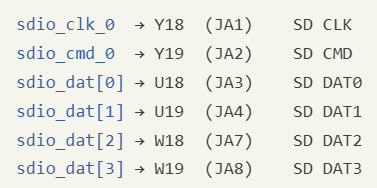
The SD card is connected via a PMOD SD card adapter providing a 3.3V supply rail, consistent with the LVCMOS33 IO standard used throughout the constraint file. The PMOD JA pin assignment used throughout the hardware validation is as follows.
Compilation on the PS ARM core
Rather than cross-compiling test binaries on the development server and transferring them to the board, the test binary was compiled directly on the PYNQ-Z2 ARM Cortex-A9 using the native GCC toolchain already present in the PYNQ Linux environment (gcc -O1 -Wall -o sdio_test sdio_tests_pynq.c sdiodrv.c pynq_bsp.c -I.). This eliminated the need for a separate cross-compilation toolchain setup, reduced the iteration cycle between driver changes and test runs, and confirmed that the binary is compatible with the exact runtime environment in which it executes.
Stage 1 and 2: clock and command line integrity
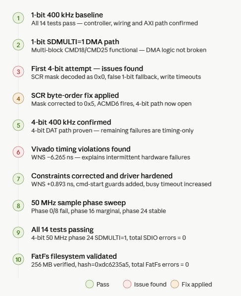
Reading the sd_phy register immediately after bitstream load confirmed the controller clock at 400 kHz before any card command was issued. CMD0 and CMD8 both completed within expected timing bounds. The CMD8 pattern echo (0xA5) was returned correctly, confirming physical card presence and 3.3V voltage compatibility.
Stage 3: full initialisation — hardware-vs-simulation differences observed
Three specific differences from simulation were observed and documented during sdio_init(), as anticipated in the verification plan.
- The ACMD41 poll loop iterated significantly more times on cold hardware than in simulation, consistent with the real card requiring time to complete its internal power-up sequence before asserting OCR bit 31. This is expected behaviour and not a failure.
- The SCR register reported 4-bit bus width support on real hardware, with the bus-width mask decoding to
0x00000005. This caused ACMD6 to fire and the host PHY to switch to 4-bit mode — a transition that did not occur in simulation because the simulation model initialised the SCR bus-width field to zero. Observing this transition confirmed that the 4-bit data path is physically wired and functional.
SCR bus-width register: byte ordering through the AXI FIFO path
The SCR register is delivered by ACMD51 as two 32-bit words through the AXI FIFO. Each word arrives little-endian — the least significant byte first. The SD specification, however, defines SCR byte significance in the opposite order: SCR[0] is the most significant byte of the first word. The original driver stored the bytes in FIFO memory order rather than SD register order, which placed the bus-width field at the wrong byte index. The decoded bus-width mask read as 0x00000000, causing the driver to conclude the card did not support 4-bit mode and fall back silently to 1-bit operation. On real hardware with a real SD card, this prevented ACMD6 from firing entirely.
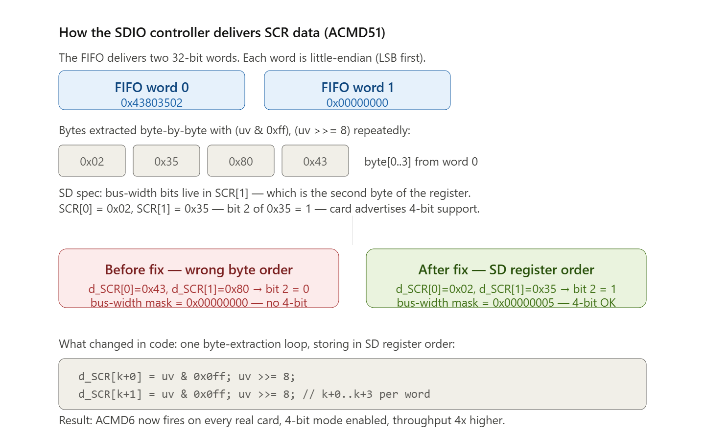
After correcting the byte extraction sequence to store in SD register order, the mask decoded as 0x00000005, ACMD6 fired, and the host PHY switched to 4-bit mode. This transition — absent in simulation because the model initialised the SCR field to zero — was one of the three hardware-vs-simulation differences the verification plan had predicted would require explicit documentation.
Stage 4: C-based test suite on real hardware — issues found
Running the fourteen-test suite on hardware without further driver changes revealed intermittent CMD24 write failures across multiple test cases. The error codes observed were SDIO-WRITE -> ERR: 04418318 with card status sd_data/R1: 00000900. The failures were non-deterministic: some runs of the same test would pass while others would fail, which immediately ruled out a deterministic RTL bug and pointed toward a timing or sequencing issue in the software path.
The failures appeared across TC05 (single block write/readback), TC06 (multi-block write/readback), TC08 (repeated transfer stress), TC10 (adversarial data patterns), TC13 (recovery after invalid request), and TC14 (scratch range integrity sweep). Read-only tests — TC03, TC04, TC11, TC12 — completed correctly throughout, which confirmed that the receive path was functional and narrowed the failure domain to the write sequencing.
Vivado static timing analysis provided the structural explanation. Before SDIO-specific timing constraints were applied, Vivado reported WNS = −6.265 ns and TNS = −177.5 ns on SDIO input paths. The failing paths involved SDIO DAT inputs being captured by registers clocked by clk_fpga_0, a PS-generated clock that is not a valid timing object until after link_design. Standard XDC files are evaluated before link_design, meaning that any constraint referencing clk_fpga_0 in the XDC would silently fail to apply, leaving the SDIO paths unconstrained and exposing the underlying routing delays as setup violations. This is the mechanistic reason why the simulation passed without error while the real board produced intermittent failures: behavioural simulation does not model FPGA placement and routing delay.
Constraint correction and timing closure
Closing timing on the SDIO paths required two changes. First, SDIO multicycle path constraints were moved from the XDC file into a Tcl implementation hook (apply_sdio_io_multicycle.tcl) invoked after link_design, at which point clk_fpga_0 is a valid timing object. A virtual SDIO timing clock was created to serve as the reference for board-interface analysis of the CMD and DAT output paths.
Second, the output hold multicycle exception required the -end flag to specify endpoint-clock edge adjustment. Without -end, Vivado adjusted the wrong clock edge for paths ending at the virtual SDIO clock, producing a false hold violation of WHS = −387.744 ns. Adding -end corrected the edge selection and the hold violation resolved immediately. The constraint applied was set_multicycle_path -hold 2 -end -from $tristate_regs -to $sdio_pins. The difference between -hold 2 and -hold 2 -end is a single token, but it is critical: for any multicycle hold constraint on an output path terminating at a virtual clock, the endpoint semantics must be specified explicitly or Vivado will apply the relaxation to the source side.
After applying the corrected constraints and regenerating the bitstream, Vivado reported: WNS = +0.893 ns, TNS = 0.000 ns, WHS = +0.037 ns, THS = 0.000 ns. The design met timing and bitstream generation completed successfully.
Driver hardening for the Linux AXI-Lite polling path
With timing closed, a class of intermittent failures remained at higher clock speeds that was not explained by FPGA timing violations. Investigation identified a software race condition specific to the PYNQ Linux userspace path. The ARM Cortex-A9 can issue an AXI-Lite read to the SDIO status register within nanoseconds of having issued a command write. In some cases the driver read the previous command's idle status before the newly-issued command had propagated through the AXI fabric and updated the controller status registers. This produced three distinct failure modes: FIFO data read before the RX buffer was valid; a subsequent command issued while the previous was still executing; and a completed command that was never seen, triggering a spurious timeout.
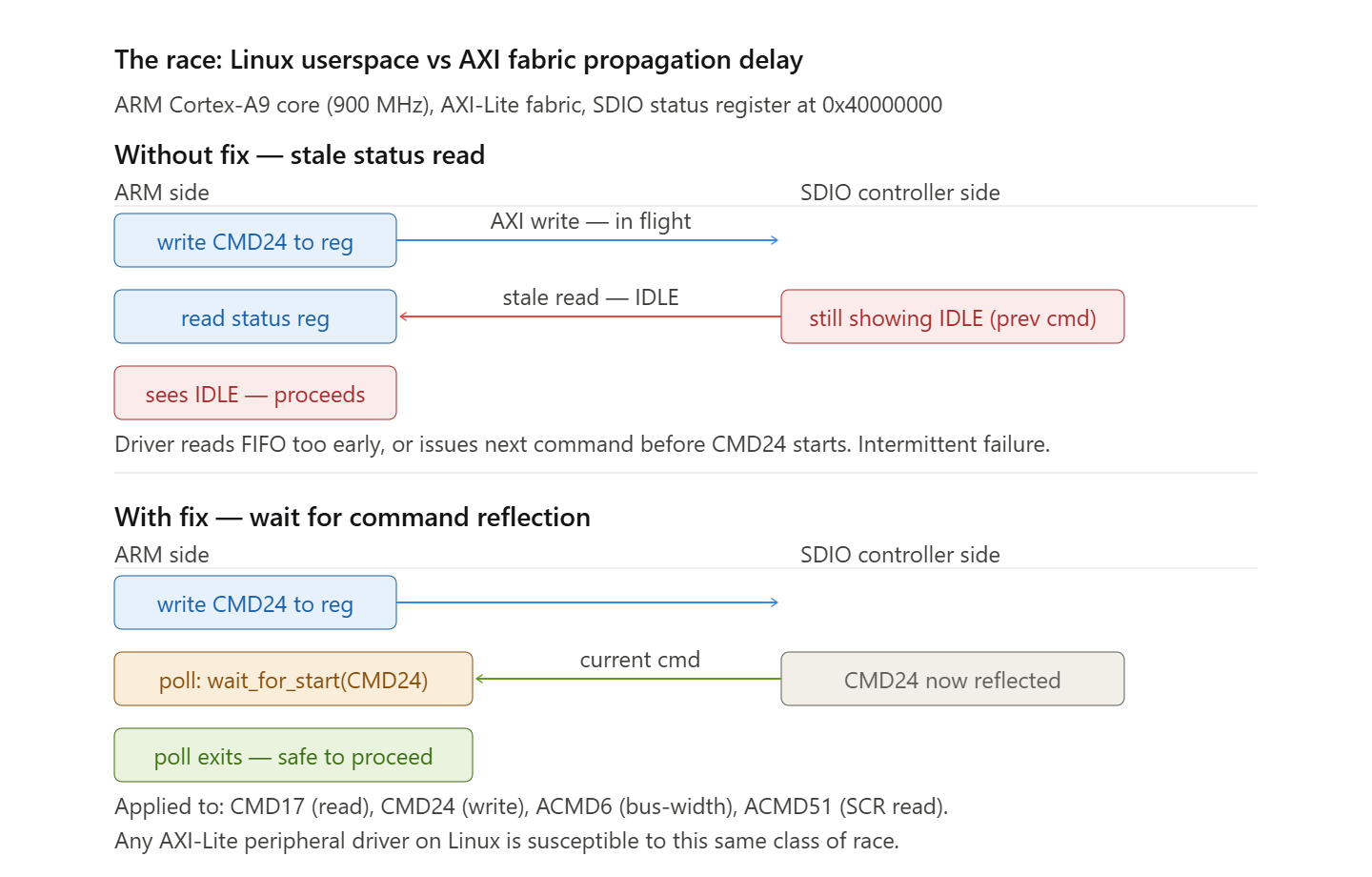
The fix was the addition of a sdio_wait_for_transfer_start() helper function, which polls the controller status register until it reflects the command that was most recently issued before allowing the driver to proceed. This guard was applied to CMD17 (single block read), CMD24 (single block write), ACMD6 (bus-width switch), and ACMD51 (SCR read). The rationale is identical in each case: the ARM core must not take any action that depends on the command having started until the controller confirms the command is visible in its own status.
Three further changes addressed write reliability specifically. The busy timeout was increased from 100,000 to 50,000,000 cycles to accommodate the real SD card's internal programming time during write-heavy test sequences — the original value was calibrated for simulation, where the model responds in a single cycle. A post-write CMD13 status check was added after each CMD24 write, creating a synchronisation point that prevents the driver from issuing a subsequent command while the card is still internally programming the previous sector. Finally, sdio_write_block() was split into an inner function and a public wrapper that retries once on a transient failure, which is safe because writing the same 512-byte payload to the same sector is idempotent.
Sample phase characterisation at 50 MHz
The 50 MHz operating point required explicit sample phase selection. The controller supports four legal phase values in this non-SERDES/non-DDR build: 0, 8, 16, and 24. Each was tested across the full fourteen-test suite. Phases 0 and 8 failed consistently. Phase 16 produced intermittent read failures, placing it in the marginal category. Phase 24 passed all fourteen tests on every run. This phase sensitivity is expected behaviour for a source-synchronous interface at this frequency: the valid sampling window narrows as the clock rate increases, and only the phase alignment that places the sample point within the card's data valid window produces reliable results. For this PYNQ-Z2 PMOD path, that alignment is at phase 24. The validated driver encodes this explicitly as PYNQ_SDIO_TARGET_PHASE = 24u with a comment documenting the phase sweep evidence.
The validated operating point for this PYNQ-Z2 PMOD non-SERDES non-DDR build is 4-bit mode, 50 MHz clock, sample phase 24, SDMULTI = 1, and post-write CMD13 status checking enabled. With the corrected constraints and hardened driver in place, all fourteen test cases passed with zero errors. Initialisation output confirmed the validation operating configuration.
Stage 5: FatFs filesystem-level validation. With block-level access confirmed, FatFs filesystem tests were executed using the same board setup. Tests covered f_mkfs format, mount of an existing filesystem, directory creation, small file write/read/compare, 64 MB large file write/read/verify, 256 MB large file write/read/verify, 512-file runs, rename and delete operations, unmount/remount, and post-remount verification. All tests passed with zero filesystem errors. These results close Stage 5 as stated in the verification plan, confirming the full path from application code through the diskio.c vtable through sdiodrv.c to the physical SD card and back
Test Matrix Automation and Stability Testing
To avoid relying on single-run pass/fail evidence, a board-side Python automation suite was developed and executed directly on the PYNQ. Two scripts work together to provide both coverage and repeatability evidence.
| run_sdio_matrix.py | Sweeps 1-bit and 4-bit modes, SDMULTI = 0 and SDMULTI = 1, six clock rates from 400 kHz to 50 MHz, and four sample phases at 50 MHz. For each configuration it patches the relevant constants in sdiodrv.c, recompiles with the board’s native GCC, runs the full 14-test suite, and captures a CSV/Markdown log. Produces the signoff matrix results shown below. |
| run_sdio_soak.py | Takes the signoff matrix and repeats it N times, classifying each configuration as STABLE (passed every run), MARGINAL (passed some runs), or FAIL (failed every run). Distinguishes a genuinely reliable operating point from one that happened to pass once. Soak results are shown in the stability table below. |
Signoff Matrix Results
The signoff matrix covers 400 kHz through 25 MHz at sample phase 16 and 50 MHz at sample phase 24, across all bus-width and SDMULTI combinations — 24 configurations in total. Every configuration passes the full 14-test suite with zero SDIO errors.
| Width | SDMULTI | Clock | Phase | Result | Errors |
|---|---|---|---|---|---|
| 1 | 0 | 400 kHz | 16 | PASS | 0 |
| 1 | 0 | 1 MHz | 16 | PASS | 0 |
| 1 | 0 | 5 MHz | 16 | PASS | 0 |
| 1 | 0 | 12 MHz | 16 | PASS | 0 |
| 1 | 0 | 25 MHz | 16 | PASS | 0 |
| 1 | 0 | 50 MHz | 24 | PASS | 0 |
| 1 | 1 | 400 kHz | 16 | PASS | 0 |
| 1 | 1 | 1 MHz | 16 | PASS | 0 |
| 1 | 1 | 5 MHz | 16 | PASS | 0 |
| 1 | 1 | 12 MHz | 16 | PASS | 0 |
| 1 | 1 | 25 MHz | 16 | PASS | 0 |
| 1 | 1 | 50 MHz | 24 | PASS | 0 |
| 4 | 0 | 400 kHz | 16 | PASS | 0 |
| 4 | 0 | 1 MHz | 16 | PASS | 0 |
| 4 | 0 | 5 MHz | 16 | PASS | 0 |
| 4 | 0 | 12 MHz | 16 | PASS | 0 |
| 4 | 0 | 25 MHz | 16 | PASS | 0 |
| 4 | 0 | 50 MHz | 24 | PASS | 0 |
| 4 | 1 | 400 kHz | 16 | PASS | 0 |
| 4 | 1 | 1 MHz | 16 | PASS | 0 |
| 4 | 1 | 5 MHz | 16 | PASS | 0 |
| 4 | 1 | 12 MHz | 16 | PASS | 0 |
| 4 | 1 | 25 MHz | 16 | PASS | 0 |
| 4 | 1 | 50 MHz | 24 | PASS | 0 |
The highlighted row is the validated production operating point. At 50 MHz, phases 0 and 8 failed consistently during the sweep; phase 16 was marginal. Phase 24 passed on every run and is the only reliable 50 MHz operating point for this PYNQ-Z2 PMOD build.
A single matrix pass confirms all configurations pass. To confirm they pass reliably, the signoff matrix was repeated five times using run_sdio_soak.py.
Soak Stability Results
24 / 24 configurations STABLE — 0 MARGINAL — 0 FAIL. 120 complete test-suite executions (24 configurations × 5 runs) with zero failures.
| Width | SDMULTI | Clock | Phase | Stability | Passes / Runs | Pass rate |
|---|---|---|---|---|---|---|
| 1 | 0 | 400 kHz | 16 | STABLE | 5 / 5 | 100% |
| 1 | 0 | 1 MHz | 16 | STABLE | 5 / 5 | 100% |
| 1 | 0 | 5 MHz | 16 | STABLE | 5 / 5 | 100% |
| 1 | 0 | 12 MHz | 16 | STABLE | 5 / 5 | 100% |
| 1 | 0 | 25 MHz | 16 | STABLE | 5 / 5 | 100% |
| 1 | 0 | 50 MHz | 24 | STABLE | 5 / 5 | 100% |
| 1 | 1 | 400 kHz | 16 | STABLE | 5 / 5 | 100% |
| 1 | 1 | 1 MHz | 16 | STABLE | 5 / 5 | 100% |
| 1 | 1 | 5 MHz | 16 | STABLE | 5 / 5 | 100% |
| 1 | 1 | 12 MHz | 16 | STABLE | 5 / 5 | 100% |
| 1 | 1 | 25 MHz | 16 | STABLE | 5 / 5 | 100% |
| 1 | 1 | 50 MHz | 24 | STABLE | 5 / 5 | 100% |
| 4 | 0 | 400 kHz | 16 | STABLE | 5 / 5 | 100% |
| 4 | 0 | 1 MHz | 16 | STABLE | 5 / 5 | 100% |
| 4 | 0 | 5 MHz | 16 | STABLE | 5 / 5 | 100% |
| 4 | 0 | 12 MHz | 16 | STABLE | 5 / 5 | 100% |
| 4 | 0 | 25 MHz | 16 | STABLE | 5 / 5 | 100% |
| 4 | 0 | 50 MHz | 24 | STABLE | 5 / 5 | 100% |
| 4 | 1 | 400 kHz | 16 | STABLE | 5 / 5 | 100% |
| 4 | 1 | 1 MHz | 16 | STABLE | 5 / 5 | 100% |
| 4 | 1 | 5 MHz | 16 | STABLE | 5 / 5 | 100% |
| 4 | 1 | 12 MHz | 16 | STABLE | 5 / 5 | 100% |
| 4 | 1 | 25 MHz | 16 | STABLE | 5 / 5 | 100% |
| 4 | 1 | 50 MHz | 24 | STABLE | 5 / 5 | 100% |
The highlighted row is the production operating point. Phases 0 and 8 at 50 MHz were classified FAIL; phase 16 was classified MARGINAL — independently confirming the manual phase sweep findings.
Signoff Matrix Results
The signoff matrix covers configurations expected to pass: 400 kHz through 25 MHz at sample phase 16, and 50 MHz at sample phase 24, across all bus-width and SDMULTI combinations. All 24 configurations pass with zero SDIO errors.
The final row is the validated production operating point. Phase 0 and phase 8 at 50 MHz failed consistently during the matrix sweep. Phase 16 at 50 MHz was marginal — intermittent read failures on some runs. Phase 24 passed on every run, confirming it as the only reliable 50 MHz operating point for this PYNQ-Z2 PMOD build.
Test Case Coverage
The block-level test suite comprises fourteen test cases exercised on every configuration in the matrix. The table below documents what each test case covers and the specific commands and conditions it exercises.
| TC | Test | Commands | What is verified |
|---|---|---|---|
| TC01 | SDIO initialisation | CMD0, CMD8, ACMD41, CMD2, CMD3, CMD9 | sdio_init() completes; OCR, RCA, CSD parsed correctly |
| TC02 | Card information validity | — | OCR voltage window, RCA assigned, block size 512 B, sector count non-zero, card type SD |
| TC03 | Single block read | CMD17 | Data changes between sectors; first 16 bytes printed for manual inspection |
| TC04 | Repeated single block read | CMD17 × 2 | Two consecutive reads to the same sector return identical data |
| TC05 | Single block write / readback | CMD24, CMD17 | Written pattern matches readback byte-for-byte |
| TC06 | Multi-block write / readback | CMD25, CMD18 | Two-sector write and read; byte-exact compare across both sectors |
| TC07 | Invalid argument handling | — | NULL driver pointer, zero block count, NULL buffer — all rejected without hang or crash |
| TC08 | Repeated transfer stress | CMD24 / CMD17 × 8 | Eight iterations with a different seed per sector; all pass |
| TC09 | Multi-sector boundary transition | CMD24 × 2, CMD17 × 2 | Last byte of sector N and first byte of sector N+1 verified independently |
| TC10 | Adversarial data patterns | CMD24 / CMD17 | Patterns 0x00, 0xFF, 0xAA, 0x55, walking ones, walking zeroes — all read back correctly |
| TC11 | Neighbour sector preservation | CMD24 to N; CMD17 to N−1, N+1 | Write to sector N does not corrupt adjacent sectors N−1 or N+1 |
| TC12 | Sector 0 preservation | CMD24 to 0x1001–0x1017; CMD17 to 0x0000 | Scratch writes to sectors 0x1001–0x1017 leave sector 0 (MBR) unchanged |
| TC13 | Recovery after invalid request | Zero-count read, then CMD24 / CMD17 | Controller recovers cleanly; subsequent valid operations succeed |
| TC14 | Scratch range integrity sweep | CMD24 / CMD17 × 16 | 16 sectors from 0x1040; unique seed per sector; every sector matches on readback |
Final result across the signoff matrix: 14 / 14 tests pass on all 24 configurations. Total SDIO errors = 0.
Conclusion
The SDIO controller has been functionally validated on the PYNQ-Z2 PMOD interface through both block-level and filesystem-level testing. The work delivered what the hardware validation plan set out to achieve: evidence that the same integration that passes simulation survives contact with a real SD card, a real AXI bus, and real FPGA timing. The issues found along the way — SCR byte ordering, AXI-Lite polling races, SD card busy handling, FPGA timing violations, and multicycle constraint semantics — were each resolved and documented. The pynq_sdio_project standalone repository is structured to be imported as a git submodule into MegaSoC or any other SoC Labs project without modification.
Project Milestones
Do you want to view information on how to complete the work stage ""
or update the work stage for this project?
-
RTL Verification
Design FlowTarget DateCompleted Date- Verifying the RTL as integrated — not the IP in isolation
- Confirming the RTL parameters are set correctly for the target build
- Confirming the RTL synthesises and meets timing on the target part
- Confirming the RTL interfaces (AXI-Lite control, AXI HP0 DMA) behave correctly when driven by real ARM software
- Identifying and resolving any integration-level RTL issues found during bring-up
Result of WorkAt integration level, all 14 C-based test cases passed. The SDIO controller can read and write data correctly — 4-bit 50 MHz SDMULTI=1 confirmed stable. SD card controller is active and verified.
-
Simulation
Design FlowTarget DateCompleted DateResult of WorkHardware bring-up directly replaced simulation as the primary correctness check. Three issues were found that simulation would not have caught: FPGA routing timing violations, AXI-Lite polling race conditions, and SCR byte-order behaviour on a real SD card.
-
Synthesis
Design FlowTarget DateCompleted Date- Vivado 2024.1 synthesised the 17 synthesisable SDIO RTL files plus the PYNQ-Z2 top-level wrapper targeting xc7z020clg400-1
- Block design connects Zynq-7000 PS to SDIO IP over AXI-Lite (control) and AXI HP0 (DMA)
Result of WorkSynthesis completed successfully. No unresolved elaboration errors. RTL parameter issues (
OPT_HWRESET,OPT_LITTLE_ENDIAN) identified and resolved at this stage before implementation. Was able to generate bitstream successfully. -
Getting Started
Design FlowTarget DateCompleted DateProject scope: Integration of the ZIP CPU SDIO Controller as a submodule of MegaSoC project.
Verification Target: PYNQ-Z2 FPGA board with SD card and Synopsys VIP simulation model
Identification and understanding of the SDIO Controller software stacks: sdiodrv.c --> diskio.c vtable --> FatFs
Perform C based Integration testing to check compatibility if ZIP CPU with MegaSoCResult of WorkZIP CPU SDIO Controller driver is verified with its own simulation model, standalone FPGA project has been created to verify the correctness of the drivers with real SD card and verified against Synopsys VIP card model as well.
All the tests cases were passed. And a new repo has been created based on the ZIP CPU SDIO controller RTL files (SoC-Labs/sdio-controller) now this is referenced as a submodule in MegaSoC-Tech, which is a submodule in MegaSoC project.
sdio-controller can be used any future projects by referencing it as submodule.
 Shiva Sangati
Research Hardware Engineer at University of Southampton
Submitted on
Comments
Milestones
Thank you for updating the milestones on this project. Reading the conclusion is could be seen that this project is coming towards a point where it will be used in other projects. Does this mean that this project had no further milestones or are their any planned?
John.
To clarify — the standalone …
To clarify — the standalone `pynq_sdio_project` was scoped specifically for FPGA validation purposes, containing only the RTL files needed to verify the controller in isolation on the PYNQ-Z2. Now that functional validation is complete, this will be processed for SoC flow along with the MegaSoC project.
Add new comment
To post a comment on this article, please log in to your account. New users can create an account.