Fast-kNN: A hardware implementation of a k-Nearest-Neighbours classifier for accelerated inference
Project Motivation and Goals
The k-Nearest-Neighbours (kNN) algorithm is a popular Machine Learning technique that can be used for a variety of supervised classification tasks. In contrast to other machine learning algorithms which "encode" the knowledge gained from training data to a set of parameters, such as weights and biases, the parameter set of a kNN classifier consists of just labelled training examples. Classification of an unlabelled example takes place by calculating its Euclidean distance (or any other type of distance metric) from all the stored training examples. The label of the unknown example is determined by the majority of the labels of the k closest examples.
In contrast to other Machine Learning methods, kNN classification doesn't require an explicit training phase, which makes it a potential candidate for learning directly from the data captured by an embedded system. However, the computation of the distance metrics between a new unclassified example and the labelled examples stored as the classifier's parameter set acts as a bottleneck in the classification process, if it is implemented in software. Through the development of dedicated hardware for calculating the required distance metrics, it is possible to reduce inference time.
The goal of this project is to build a hardware implementation of a kNN classifier that can achieve reduced inference time when compared to a kNN classifier implemented fully in software, through the parallelisation of distance metric computations. The project has an educational purpose and it expected that by its completion, the contributors will have gone through the complete design cycle of a SoC.
Design Specification
The first step in defining the design specification for the accelerator was to determine the type of data that need to be processed by it. The Fashion-MNIST dataset has been selected as the primary data source. Therefore, the accelerator should be able to handle grayscale image vectors with a size of 28 x 28 pixels. We assume that some of these images will be labelled (training set), while some of them won't (test set). The accelerator should help with computing the distance between all the labelled images and each unknown image in the unlabelled set.
Data to be processed: N 28 x 28 8-bit (grayscale) labelled image vectors and M unlabelled image vectors, stored in SRAM.
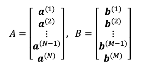
Image vectors a(i), b(j) have D elements, where D = 28 x 28 = 784. Each element is represented as an 8-bit unsigned integer value. If N = 200 and M = 50, the total storage requirements for matrices A and B are:
N x 785 + M x 784 = 200 x 785 + 50 x 784 = 196,200 bytes, which is approximately equal to 192 kB. It is assumed that one byte of storage is required for storing every label. This is the reason why the number of labelled examples N is multiplied by 785 and not 784.
We would like to compute the Squared Euclidean distance between each pair of vectors a(i), b(j). This computation is given by the sum of 3 dot products, as shown below:
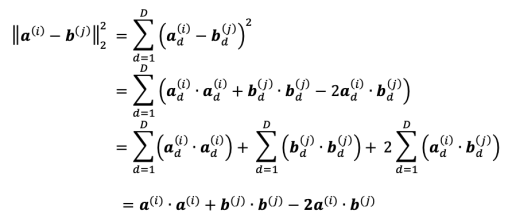
The self-dot products a(i)⋅a(i) and b(j)⋅b(j) can only be computed once and then reused for another computation.
Design Rationale
Constraints introduced by the SoC infrastructure
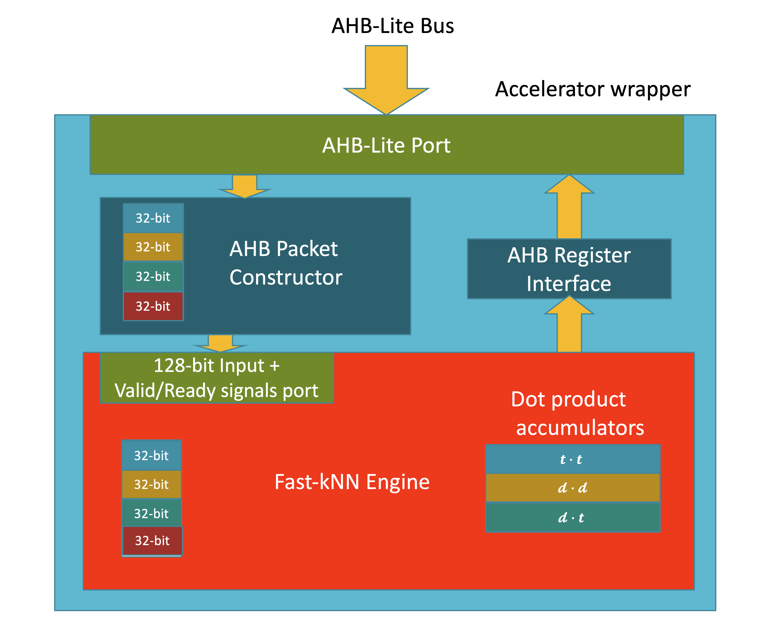
The nanosoc infrastructure provided by SoCLabs was used as the core of the design. At the early design stages, it was decided not to use a DMA peripheral for writing/reading data to/from the accelerator engine to keep things simple. Therefore, all the data movements to/from the accelerator were happening through the AHB-Lite Bus.
Accelerator Dataflow
The accelerator's input data consist of high-dimensional image vectors. In contrast, its output data consist of just three scalar values. In addition, the rate at which data need to be written to the engine is much higher than the rate at which computed values need to be moved out. The above two observations indicate that the accelerator's dataflow is highly asymmetric. Writing a complete image vector to the accelerator engine instantaneously is not possible due to the bus constraints. However, computing the desired dot-products can happen incrementally, using parts of the image vectors delivered as packets.
The size of each input packet was set arbitrarily to 128 bits (16 bytes). An image vector with 784 byte long elements, can be split into 784 / 16 = 49 packets. The AHB-Lite Bus can deliver a 32-bit data word, which means that 4 write operations are required to create a packet of 128 bits.
I/O Ports
Input port:
- 128-bit Valid/Ready signal port
Output port:
- Register interface for reading the contents of the dot product accumulators and monitoring internal control/status registers.
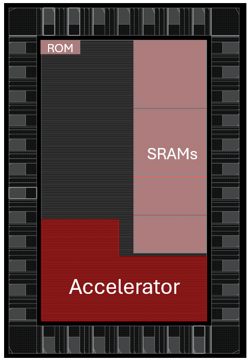
System overview
To properly interface the Fast-kNN engine with the AHB-Lite bus, the accelerator wrapper IP provided by SoCLabs was used. Data words delivered through the AHB-Lite bus are passed to the AHB Packet Constructor which packages them into 128-bit packets. These packets are then passed to the engine though a valid-ready handshake. Reading the accumulator registers that hold the results of the computation required the use of the AHB Register Interface IP.

Fast-kNN Engine
The Fast-kNN accelerator consists of the following parts:
- A byte long buffer with a depth of 784 elements, whose purpose is to store a complete unlabelled image vector.
- A byte long buffer with a depth of 16 elements that temporarily holds a data packet from a labelled image.
- Three 32-bit accumulator registers that hold the computed dot products. The contents of these registers are updated incrementally as new data packets become available.
- A 3-bit control register, where each bit has the following role:
- Bit 0 - Packet data ready flag. This flag is pulled low when the transfer of the input data packet from the packet constructor to the engine is complete and the dot product computation can begin.
- Bit 1 - Priming mode flag. This flag is pulled low when the unlabelled image buffer becomes full.
- Bit 2 - Software reset bit
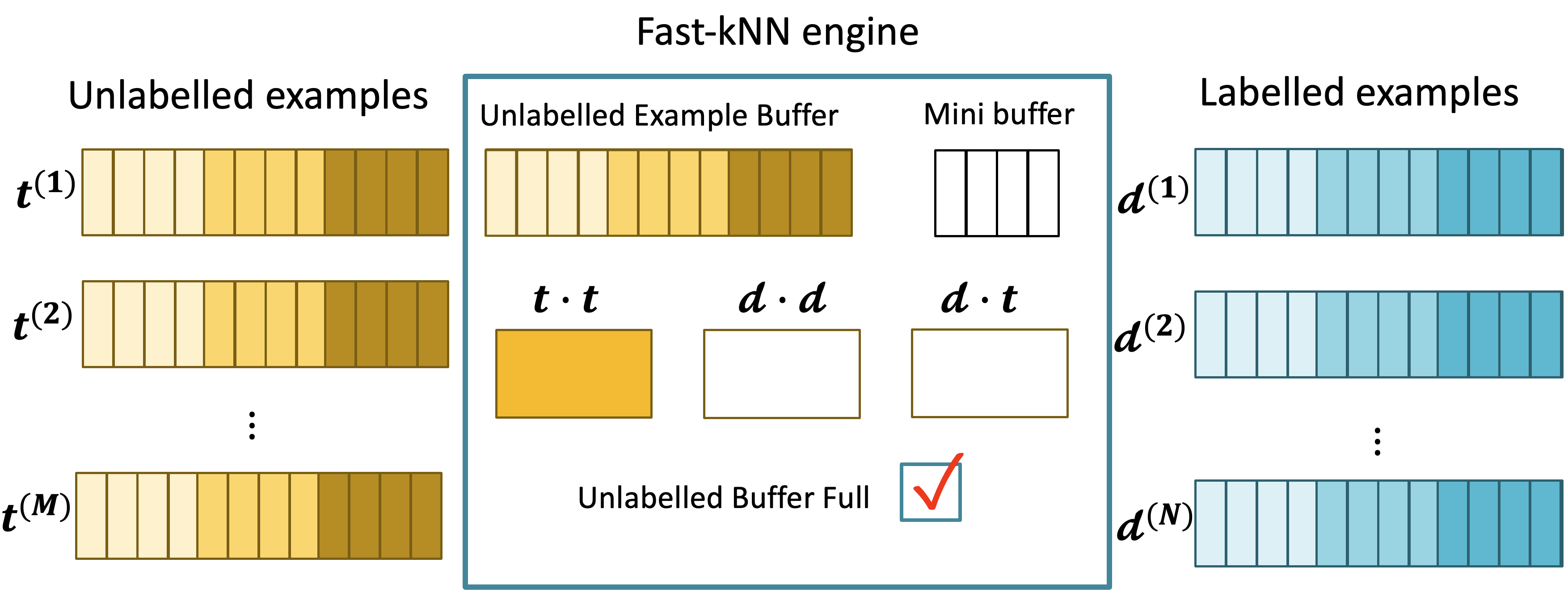
After a reset, all data registers are empty and the priming mode flag is high. Delivered packets are written to the unlabelled image buffer and the self-dot product for the unlabelled image is incrementally accumulated. When a complete unlabelled image vector has been written to the engine, the priming mode flag is pulled low. Packets from a labelled image can then be delivered to the engine for the computation of the other two dot products to take place. Once all elements of the labelled image vector have been delivered to the engine, the accumulated values can be read through the AHB register interface. The same process is repeated for all labelled images. Before writing a new labelled image to the engine, all the data registers need to be cleared and the priming mode flag needs to be pulled high.
Backend Flow
Accelerator Synthesis
Synthesis was run using Cadence Genus, using the scripts provided by SoClabs. The final accelerator area using a packet width of 128 was 139,000 µm2. Whilst running synthesis it was found that there was an unsynthesisable construct in the main accelerator engine, which was due to an incorrect definition of an asynchronous reset. This was fixed by ensuring the reset was in the sensitivity list of the always block and an if/else statement was used for the reset case.
Floor Planning
The relative placement of the accelerator to the rest of the SoC required partitioning the die into two power domains, one for the SoC and one for the accelerator, allowing for direct external measurement of the power used by the accelerator. The percentage of the entire ASIC tacken up by the accelerator was about 18%, this was mostly due to the large number of registers used within the accelerator.
Tapeout
The final GDS design has been sent off for fabrication. The final specs for the design are:
- Max clock frequency: 240 MHz
- Accelerator Power consumption (20% activity): 55.1 mW
- Total SoC Power consumption (20% activity): 146.5 mW
- Leakage Power: 39 µW
- Internal Memory: 48 kB (16 kB Instruction and Data memory + 2x 8 kB accelerator memory)
- Supply voltage: 1.2 V
- Interfaces: UART, FT1248, SWD
- GPIO: 8 pins x 2 ports
Implementation of software tests on the SoCLabs demo board
As well as confirming the silicon implementation was successful, an important aim of the software and test board was to capture statistics about the average time the ASIC implementation requires to run all the dot product calculations while running kNN inference for an unlabelled image. Carrying out the same computational load in software, without using the Fast-kNN engine was set as the comparison baseline.
| Time required to compute distance metrics (ms) | |
|---|---|
| In software (on nanosoc's M0 core) | 10,500 |
| With Fast-kNN engine | 3.5 |
The overall speedup observed was an approximate reduction in average compute time by x3000. However, the implementation of the computations in software could be implemented in a more efficient way, which could decrease the actual speedup obtained by Fast-kNN engine.
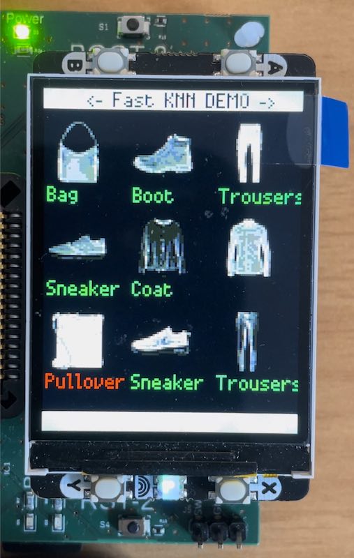
Demo on SoCLabs testboard
Implementation of a demo displaying the classification of a subest of FashionMNIST test images using the Fast-kNN engine on the screen of the SoCLabs test board.
To make the test board at a low cost the interface is shared between accessing the micro-SD card contents and writing to the board's screen through the shared SPI bus. This compromises Fast-kNN application as it is currently not possible to switch between loading data from the SD card and printing content to the display to keep the engine operating effectively. Therefore, all the the data is preloaded from the micro-SD card to the RP2040 on chip memory, which restricts the number of train/test images to 160 and 27 respectively.
A video showing the demo running on the board can be found here.
Project Milestones
Do you want to view information on how to complete the work stage ""
or update the work stage for this project?
-
First abstract description of project goals
Target DateCompleted DateRough outline of the project's goals, hardware accelerator idea and motivation.
-
Architectural description and Familirisation with design tools
Target Date- Specify the number format used for the arithmetic operations of the accelerator (i.e. 8-bit unsigned integers for grayscale images).
- Select the distance metric used for kNN classification (i.e. Euclidean distances).
- Determine the type of building blocks (i.e. adders, multipliers) required to perform the arithmetic operations.
- Capture the architectural design in block diagram format, specifying the necessary inputs, outputs, registers and the overall data flow.
- Complete the lab exercises from the "Introduction to SoC design" course to gain familiarity with Xilinx Vivado.
-
Initial RTL Implementation
Target DateCompleted DateFamilirisation with SoCLabs Accelerator Wrapper IP
Implementation of Packet constructor wrapper for writing 128-bit dat packets to the device
-
Implementation of AHB Register interface
Target DateCreate register interface for reading the contents of accumulator registers
-
Addition of DMA peripheral
Target Date -
Software tests
Target DateImplement software tests to check the accelerator's functionality at extreme cases.
-
Final RTL submission
Target DateCompleted DateSubmit the final design, integrated with nanoSoC for backend flow
-
Synthesis
Design FlowTarget DateCompleted DateRun synthesis and formal equivalence checks
-
Floor Planning
Design FlowTarget DateCompleted Date -
Clock Tree Synthesis
Design FlowTarget DateCompleted DateClock tree synthesis and timing optimisation
-
Timing closure
Design FlowTarget DateCompleted Date -
DRC
Target DateCompleted DateCheck DRC and fix any errors
-
Tape Out
Design FlowTarget DateCompleted DateSubmit for tapeout to europractice TSMC 65nm mini ASIC shuttle
-
Inference statistics capture
Target DateCompleted DateImplementation of software tests on the SoCLabs demo board
The aim of the software tests were to capture statistics about the average time required to run all the dot product calculations while running kNN inference for an unlabelled image. Carrying out the same computational load in software, without using the Fast-kNN engine was set as the comparison baseline.
Average time required for computing Euclidean distances between 1 unlabelled image and 160 labelled images Time required to compute distance metrics (ms) In software (on nanosoc's M0 core) 10,500 With Fast-kNN engine 3.5 The overall speedup observed was approximately a reduction in average compute time by x3000. However, the implementation of the computations in software could perhaps be implemented in a more efficient way, which could decrease the actual speedup obtained by Fast-kNN engine.
-
Demo on SoCLabs test board
Target DateCompleted DateImplementation of a demo displaying the classification of a subest of FashionMNIST test images using the Fast-kNN engine on the screen of the SoCLabs test board.
Because of a conflict between accessing the micro-SD card contents and writing to the board's screen through the shared SPI bus, it is currently not possible to switch between loading data from the SD card and printing content to the display. Therefore, all the the data are preloaded from the micro-SD card to the RP2040, which restricted the number of train/test images to 160 and 27 respectively.

Team
 Epifanios Baikas
PhD Student
at University of Southampton
Research area: Machine Learning on Resource-Constrained Embedded Systems
![]() Machine Learning
Machine Learning
![]() Hardware design
Hardware design
Submitted on
Comments
Video of the working accelerator in the test board
Hi,
It would be great to get a video of the working accelerator added to the project when you have time.
Post Tape Out Activity
There is some additional work post tape out in preparation for the testing the die within the test board. Can we capture any learning points here?
Die are back
Good news, the die are back from fabrication. How are the activities going for the tests for the die using the test board and your application to run on the test board as a demonstration?
John.
Post Tape Out Validation and Test Board
It is great to get the design off for tape out and awaiting the die back from the foundry. How are you getting on with the milestones for the post tape out validation and the use of the new nanoSoC test board?
Design Progress
As Daniel suggests, looking for the sweet spot where the SoC as a system is optimised both in data processing (calculations and their parallelism) and data movement (minimising the time where the bus is not utilised) is aiming to a point where you are able to run the calculations as fast as you can move the data.
As outlined the two aspects to consider;
1) The SoC integration issue (outside in)
2) The accelerator design (inside out)
Increasing the data processing capacity can be brute parallelism, just replication of processing blocks or data data specific optimisations, black pixels that are represented as zero which could reduce computation. Does a black pixel in the input image not add any contribution to the distance to all other class members? Holding data is changing less frequently (the unknown example) while you iterate data for say the members of a class?
Increasing utilisation of the system to move the data associated with processing. This is the SoC integration issue. How to maximise the data flowing across the bus into your accelerator. Looking at the asymmetry of data input to calculated outputs.
In this contest pathway, it is not about the ultimate design, it is about your journey in looking at optimisation strategies both in the utility of the SoC infrastructure and the application domain calculations. Perhaps when you have a next view of your design and the thoughts behind it you can share it?
Optimisation of Parrallelism
Hi Fanis,
I've see you've added some update to the architectural design of your project. And at the moment are looking to take in 4 x 8 bit words at a time. One potentially good approach to seeing how you can work on these dot products in parallel would be to use the architecture you've chosen as a starting point (2 parallel calculations of a1, a2, b1, b2) and through simulation see where your current bottleneck are. If the bottleneck is your data processing and not your data fetching, you could try increasing the number of parallel branches until you reach a point where you are able to run the calculations as fast as you can fetch data.
Taking this iterative approach can give you a good view of how to optimise your design for the nanosoc. Also if you take your current design all the way through to synthesis, you can then estimate what footprint a single dot product branch takes up. And estimate how many branches you would be able to fit in the tape out
Daniel
Vector Element Input
Hi Fanis,
With the vector input, you say you can put 4 vector inputs per 32-bit transaction. Are these all going to be from the same image and buffer them, are they going to be 2 vectors from image A and 2 from image B or will it change depending on where you are in your calculation flow?
Thanks,
David M
Patterns and how they help
Identifying both Data Patterns and Design Patterns can really help in the design phase. Look at how the data in structured in the calculations in relation to the labelled data set and unknown examples and how they interact and the implication on their storage in memory and flow across the SoC. That will help identify the Design Patterns for the IP blocks.
Data Patterns
Does the Fashion-MNIST dataset provide any natural advantages for processing. For example does the background being black mean the value 0 represents the background?
Architectural design phase
It is good to see you working through the Architectural design phase and building the conceptual understanding of the design and design space for potential alternative designs.
It is interesting to consider the flow of 32-bit words over the bus into the accelerator and how these are structured compared to the original view for the labelled and unknown examples. How you can sequence the calculations and any intermediate results you can hold. Unlike the example SHA-2 accelerator that needs data aggregated from 32-bit words before it can undertake calculation in this case you may be able to undertake calculation more efficiently.
Design Flow help
David and Daniel have added some items in the https://soclabs.org/design-flow/soc-design-contest-2023-example-flow that have some helpful questions such as can we at this stage identify and 'system bottlenecks'. Do other design decisions such as say the use of the 'reference design' constrain our design space, eg. how much data can we flow through the accelerator, what memory constrains/organisation. What area are we looking to deploy? How many calculations can we undertake in parallel? We can start to lay out questions and answers as part of conceptual understanding of a design.
How did you get on with your May 1st milestone?
Hi,
It would be great if you could let us know how you are getting on with your May 1st Milestone and if there is any help you need for planning the next milestones and support in terms of generic reference design technology or design flow environment help?
Hi, I've been having some…
Hi, I've been having some issues while trying to familiarise myself with the tools introduced by the labs of the Intro to SoC design course offered by Arm Education Media. The presented workflow introduces Xilinx Vivado and Arm Keil, both of which require a Windows environment (I think Vivado can also run on Linux). I am a Mac user and as a consequence I had trouble using the software. I have tried using the Soclabs servers, but the interface seems to become irresponsive sometimes. I have been told that this might be caused by a screensaver setting, but I still need to check.
Hopefully the advice on the…
Hopefully the advice on the local server has got you past that problem. Hopefully you can move on to the process of design. The process of design, like the design itself, can benefit from re-use. Design is a conceptual process and we often re-use techniques such as top down decomposition or bottom up. We can iterate between them to build out understanding. We can arm ourselves with questions that help rationalise the conceptual design.
In this case we have a known approach, k-Nearest-Neighbours (kNN) algorithm, and you have started to decompose this (top down). You also need to consider how you will calculate distances (bottom up). What is needed for each calculation and how does the SoC deliver that to allow the calculations to efficiently be undertaken. What are the limitations that are imposed by the SoC system and how best do we translate the mathematical algorithm onto it.
In the example accelerator we show some custom logic for performing calculations. We have data moving across the bus of the SoC and into the accelerator and results coming back out. In your example how symmetric is the data needed versus the result and does that have any implications? What is the pattern of data flowing across the bus? Asking such questions helps develop our understanding of the design. Design is as much about generating questions as it is about generating answers.
Perhaps you can share how you are developing your conceptual understanding of the Architectural Design space?
Add new comment
To post a comment on this article, please log in to your account. New users can create an account.