
Projects
Articles
Interests
Design Flow
Technology
Authored Comments
| Subject | Comment | Link to Comment |
|---|---|---|
| Collaboration |
Hi, One of the goals of SoC Labs is to help form global collaborations. It might seem odd to have a contest where you actually work with other contestants but that is something a bit unique. about this contest, it is better to work in collaboration and to share IP blocks that are re-usable across projects. John. |
view |
| Progress on nanoSoC. |
The 2023/24 version of the nanoSoC reference design has been used to tape the following projects with custom accelerators and will hopefully give you some help in developing your own project.
The die from the ASIC fabrication are back from manufacture and are being tested using the nanoSoC test board. If you need any help with your project please let us know. John. |
view |
| Data bandwidth requirements |
Hi, Do you know the data throughput requirements you are expecting for this application. If you can let us know that may help define the SoC system. John. |
view |
| Welcome to SoC Labs |
Hi, Thanks for signing up to SoC Labs. We would be happy to work with you to find any potential projects that might work for you. I see you have shared an interest in FPGA using the Xilinx platform. We have also just had two projects tape out using TSMC 65nm node for student led projects. I look forward to hearing from you. John. |
view |
| Integration of a DMA engine |
Here are the two projects that use the nanosoc reference design that have been verified through to tape out and have ASICs operational in the test board.
|
view |
| Thank you for the updated milestones |
Hi, Thanks for the updated milestones. If you need any help with the Synthesis then please let us know. John. |
view |
| 90nm tape out |
Thanks for adding the latest milestone on the synthesis using 90nm libraries. Have you obtained foundry specific libraries? |
view |
| Architectural design pattern for data movement within the SoC |
It was good to hear you confirm the Architectural design pattern for data movement within your proposed SoC. It was interesting talking through the various options:
Given the low data bandwidth requirements for you specific project you felt the DMA approach was not needed. A simple interrupt architectural design pattern with a mapping of registers within your custom hardware into the address space of the processor and accessible from the main system bus was I recall your proposed design. This will be a combination of data, status and result registers. It will be good to see how this develops. |
view |
| Using HLS4ML as a modelling tool for Architectural design |
The HLS4ML environment can use various backend tool chains for High Level Synthesis (HLS). These tools support the generation of variations of hardware implementation for an algorithm written in a high level language portable language. The benefit of High Level Synthesis is that it bridges hardware and software design domains. It was good to get some details of your design environment. As I understand things you are using the Xilinx® Vivado® High-Level Synthesis (HLS) tool chain as your backend. HLS4ML uses streams to pass data and these are mapped into implementation buffers. As with other abstractions it provides an accelerated design environment but then requires effort to optimise the hardware implementation. This can be done by developing optimization directives that direct the tool chain to refine the automated generation of the implementation. Alternatively some design teams move to use the next layer of tooling down in the design abstraction environment once they have a conceptual design. The data model for your project is relatively easy to understand. It was interesting discussing the use of the Xilinx® HLS streaming interface. We also discussed some of the challenges of moving beyond the FPGA fabric support into the full ASIC implementation flow and the subtle differences in performance of logic and memory between the two hardware instantiations. It will good to hear how things are progressing. |
view |
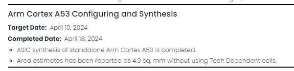
| A good example of milestones |
Here is a good example of update to a milestone to add a completion date and show progress. It comes from one of last years projects.
It shows both the Completed Date and key additional information such as the reported area with a clear statement of the inputs that this is not using a specific technology node standard cells. |
view |
Comments
Hi John,Thank you so much…
Hi John,
Thank you so much for the warm welcome to the community. Sure I would love to learn more. We can have a meeting at your convenience and discuss it. Let me know which times and dates work for you.
Add new comment
To post a comment on this article, please log in to your account. New users can create an account.