
Arm Cortex-A53 processor
There is growing interest within the SoC Labs community for an Arm A-Class SoC that can support a full operating system, undertake more complex compute tasks and enable more complicated software directed research. The Cortex-A53 is Arm's most widely deployed 64-bit Armv8-A processor and can provide these capabilities with power efficiency.
This project mirrored the 'Arm Cortex-M0 microcontroller' project in establishing a baseline capability for the Cortex-A53 processor. It is the foundation for the megaSoC reference design in the same way the Arm Cortex-M0 microcontroller project was the foundation for the nanoSoC reference design. Both foundational projects developed the core capabilities around the processor core including:
- Establishing the critical boot system
- The system debug environment
- An easy design transition from the FPGA prototyping flow to the full ASIC flow
The later involved replicating the resources available in the Zynq FPGA processing system to allow the seamless transition between FPGA and ASIC.
towards megaSoC
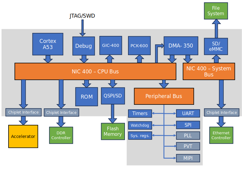
Using these foundations work will be undertaken to develop a more complete megaSoC reference design. This system will have:
- Cortex A53 processor
- High bandwidth data bus (NIC400)
- High capacity memory (DDR)
- NVM storage for deploy-ability
It will maintain resources for high data loads with configurable hardware accelerators working in combination with CPU cores under a complex software environment.
Milestone 1 - Minimum bootable subsystem
The start for this project was a minimum bootable subsystem in simulation. The idea for this subsystem is to be able to run code on the Cortex A53 and interact with the outer testbench (via UART)
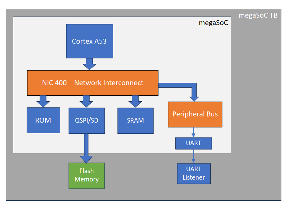
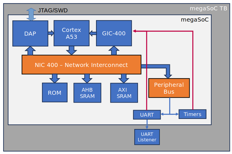
From the above image you can see the basic architecture. This has a Cortex A53 connected to a NIC-400 bus. A ROM that acts as boot rom, XiP QSPI controller for instruction memory, and SRAM as data memory. The UART is included to allow for printf statements in the C code.
The XiP QSPI is used as the entire instruction memory space, however future projects may be undertkanen to use only as a BIOS for a linux system. The rest of the linux software will be installed on external storage (either SD card or SATA capable device)
Boot Sequence
The boot sequence for the Arm Cortex A53 is more complex than the Cortex M0 and requires more care. The full information on this can be found from Arm here, which describes how to boot a Armv8-a processor.
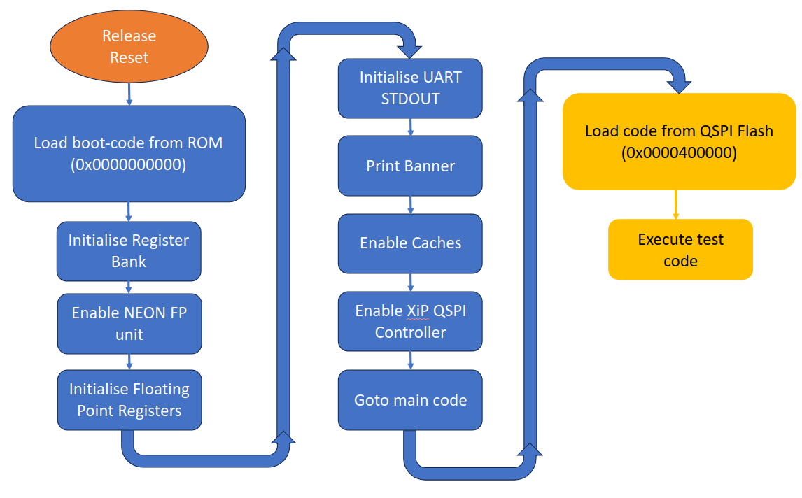
Above is a simplified boot sequence used for this project's subsystem. The boot-code (in ROM) is responsible for starting the A53 in a clean state (i.e. registers are initialised) and enables the UART communication and caches (L2 and Flash Cache) before enabling the XiP QSPI controller and then setting the execution to the Flash region.
The expected output from the ROM boot-code is as follows:
SoCLabs MegaSoC
Flash enabled... Excecuting
This first stage booting process worked as expected. However the hello_world testcode looked like it is going straight into an exception. The code is as follows:
#include "host_chassis_control.h"
#include "system.h"
#include "system_level_functions.h"
#include "uart_stdout.h"

int main(void) {
  uint32_t errors = 0;

  printf("Hello SoCLabs MegaSoC\n");

}
On execution in simulation the print message was not displayed. Further debugging was required.
A53 debugging in simulation
Debugging a complex processor like the A53 using the simulation GUI is difficult. That is why Arm processors are delivered with a Tarmac unit. These units are used in simulation to show exactly what the processor is executing, and can be very useful when debugging. The ca53_univent_follower module has to be included in the vc filelist, and the ca53_tarmac_dpi.so object must be loaded by the simulator. Exact details on how to do this are included in the README_tarmac.txt in the ca53univent directory.
The tarmac requires some libraries to be installed before use, most notable the libprotobuf.so.7 from protobuf 2.4.1. To install you can follow the steps outlined below (taken from here):
wget https://github.com/protocolbuffers/protobuf/releases/download/v2.4.1/protobuf-2.4.1.tar.bz2
tar -xvjf protobuf-2.4.1.tar.bz2
cd protobuf-2.4.1/
./configure --with-zlib --prefix=<prefix> CXX='g++ -m32 -std=c++98'
make install
WARNING
Initially this was not working, giving the message:
univent follower module: megasoc_tb.u_megasoc_chip_pads.u_megasoc_chip.u_megasoc_system.u_megasoc_tech_wrapper.u_megasoc_cpu_ss.u_cortexa53.g_ca53_cpu[0].u_ca53_cpu.u_ca53_noram.u_follower
/home/dwn1c21/SoC-Labs/megasoc_project/megasoc_tech/logical/CortexA53_1/logical/ca53univent/build_x86_32/bin/ca53_tarmac_decode: symbol lookup error: /home/dwn1c21/SoC-Labs/megasoc_project/megasoc_tech/logical/CortexA53_1/logical/ca53univent/build_x86_32/bin/ca53_tarmac_decode: undefined symbol: _ZN6google8protobuf8internal12kEmptyStringE
Error writing trace: Broken pipe
Support from Arm was requested on a way to fix this issues.
UPDATE
Following support from Arm on this issue with the tarmac module. It seems like its an issue of building the protobuf library on RHEL 8, they have supplied us with a compiled protobuf library to use (which I believe they compiled in RHEL 6) which now works. So back to debugging...
Now with the working A53 tarmac module, it could be seen that the issue was that when it changed to executing from the bootrom to the QSPI flash, there was an abort exception. After reviewing the simulation in the GUI, it could be seen there was some issue with the AHB QSPI module. As this module is not fully verified yet, it was decided to remove it for now and replace this with an AHB SRAM module (the same AHB port and range is used so that it is easy to re-instantiate the QSPI module once it is working)
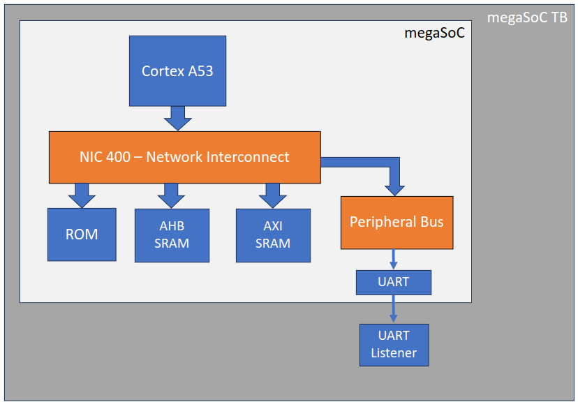
The simplified testbench structure can be seen above. This gives a successful boot. The main bootcode now looks like below:
- boot.s
.section SECURE_ROM_BOOT, "ax" .balign 8 .global Image$$ARM_LIB_STACK$$ZI$$Limit .global __main .global monitor_vectors .global __stack_multi_cpu_init .weak monitor_vectors // ------------------------------------------------------------------------------ // Core initialisation from reset state // ------------------------------------------------------------------------------ .global app_bl1_entry .type app_bl1_entry, @function app_bl1_entry: MOV x0,#0x0 MOV x1,x0 MOV x2,x0 MOV x3,x0 MOV x4,x0 MOV x5,x0 MOV x6,x0 MOV x7,x0 MOV x8,x0 MOV x9,x0 MOV x10,x0 MOV x11,x0 MOV x12,x0 MOV x13,x0 MOV x14,x0 MOV x15,x0 MOV x16,x0 MOV x17,x0 MOV x18,x0 MOV x19,x0 MOV x20,x0 MOV x21,x0 MOV x22,x0 MOV x23,x0 MOV x24,x0 MOV x25,x0 MOV x26,x0 MOV x27,x0 MOV x28,x0 MOV x29,x0 MOV x30,x0 MSR SP_EL0,x0 MSR SP_EL1,x0 MSR SP_EL2,x0 MOV sp,x0 MSR ELR_EL1,x0 MSR ELR_EL2,x0 MSR ELR_EL3,x0 MSR SPSR_EL1,x0 MSR SPSR_EL2,x0 MSR SPSR_EL3,x0 //=================================================================== // Set Vector Base Address Register (VBAR) to point to this application's vector table //=================================================================== LDR x0, =monitor_vectors MSR VBAR_EL3, x0 // EL3 sets vector base address //=================================================================== // Clear the PSTATE.A fpr enabling SError Aborts (Posion Error) //=================================================================== MSR DAIFCLR, #0x4 ISB //=================================================================== // Enable NEON and initialize the register bank //=================================================================== MRS x0, ID_AA64PFR0_EL1 SBFX x5, x0, #16, #4 // Extract the floating-point field MOV x1, #(0x3 << 20) MSR cpacr_el1, x1 MRS x1, cptr_el3 BIC x1, x1, #(0x1 << 10) // Ensure that CPTR_EL3.TFP is clear MSR cptr_el3, x1 ISB sy #ifndef NOFP FMOV d0, xzr FMOV d1, xzr FMOV d2, xzr FMOV d3, xzr FMOV d4, xzr FMOV d5, xzr FMOV d6, xzr FMOV d7, xzr FMOV d8, xzr FMOV d9, xzr FMOV d10, xzr FMOV d11, xzr FMOV d12, xzr FMOV d13, xzr FMOV d14, xzr FMOV d15, xzr FMOV d16, xzr FMOV d17, xzr FMOV d18, xzr FMOV d19, xzr FMOV d20, xzr FMOV d21, xzr FMOV d22, xzr FMOV d23, xzr FMOV d24, xzr FMOV d25, xzr FMOV d26, xzr FMOV d27, xzr FMOV d28, xzr FMOV d29, xzr FMOV d30, xzr FMOV d31, xzr #endif B __main- bootloader.c
#include "system.h" #include "qspi_flash.h" #include "cpu_asm_codes.h" #include "uart_stdout.h" #include <stdio.h> int main(void) { uint32_t errors = 0; UartStdOutInit(); printf("SoCLabs MegaSoC\n"); enable_caches(); enable_caches_el1(); printf("Flash Enabled...Booting\n"); void (*main_code)(void) = (void (*)())0x00400000; main_code(); }- hello_world.c
#include "uart_stdout.h"
#include <stdio.h>

int main(void) {
  uint32_t errors = 0;
  UartStdOutInit();

  printf("Hello SoCLabs MegaSoC\n");
  UartEndSimulation();
}
And the output we get from simulation is:
uartcapture: Generating output file logs/uart.log using MCD 00000003 @ megasoc_tb.u_uart_capture
univent follower module: megasoc_tb.u_megasoc_chip_pads.u_megasoc_chip.u_megasoc_system.u_megasoc_tech_wrapper.u_megasoc_cpu_ss.u_cortexa53.g_ca53_cpu[0].u_ca53_cpu.u_ca53_noram.u_follower
[M] 119692088.0 ()  Constructing static cortexa53 follower
[M] 119692088.0 ()  Tracing 'megasoc_tb.u_megasoc_chip_pads.u_megasoc_chip.u_megasoc_system.u_megasoc_tech_wrapper.u_megasoc_cpu_ss.u_cortexa53.g_ca53_cpu[0].u_ca53_cpu.u_ca53_noram.u_follower' to 'ca53_tarmac.0.0.0.log'
SoCLabs MegaSoC
Flash Enabled...Booting
Hello SoCLabs MegaSoC
Test Ended
$stop at time 753955 ns Scope: megasoc_tb.u_uart_capture.p_sim_end File: /home/dwn1c21/SoC-Labs/megasoc_project/verif/trace/megasoc_uart_capture.v Line: 244
xterm-256color is Not a valid terminal...
ucli% ca53_finish called
           V C S   S i m u l a t i o n   R e p o r t
Generic Interrupt Controller integration
The next step added the interrupt handling. The A53 implements a Generic Interrupt Controller ("GIC") architecture. In order to support multiple interrupts a generic interrupt controller is required. The GIC-400 from Arm is the smallest GIC from Arm. The aim with megaSoC is to focus on a design that is simple to understand and has a low cost of fabrication for academic use. The design proposed does not need support for multiple compute clusters so the GIC-400 is a good choice.
Behavioural integration is relatively straight forward. The GIC-400 has an AXI4 slave interface in order to program the interrupts once the interrupt ports are connected from GIC to CPU. In order to verify the behaviour of the GIC-400, a an APB timer is added to the peripheral subsystem to generates interrupts. The updated architectural view is below, with the red lines indicating the shared peripheral interrupt connections.
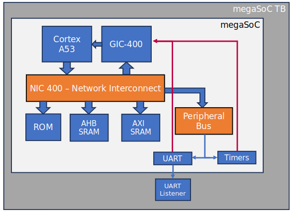
The software system for interrupt handling initialises the interrupts for the GIC-400, configuring which CPU should service the interrupt (if there are multiple CPUs/cores). Whether the interrupt is edge or level triggered, a priority level, which are initialised in the GIC distributor. The CPU needs the location of the interrupt handler configured for that interrupt, before enabling the interrupt in the GIC and enable interrupts for the CPU.
Once the interrupt is initialised, the timer is setup and there is a wait for the interrupt. The WFI instruction has not been used as if the interrupt doesn't work, the execcution will just hang, so setup a timeout function in case the interrupt is not called or serviced properly. See the below code for more detail
- gic_tests.c
#include "uart_stdout.h"
#include "sys_memory_map.h"
#include "sys_intr_map.h"
#include <stdio.h>
#include "gic400.h"
#include "CMSDK.h"
#include "irq.h"


int timer0_id_check(void);
int timer_interrupt_test_1(CMSDK_TIMER_TypeDef *CMSDK_TIMER);
static void timer_interrupt(int num, int src);

/* peripheral and component ID values */
#define APB_TIMER_PID4  0x04
#define APB_TIMER_PID5  0x00
#define APB_TIMER_PID6  0x00
#define APB_TIMER_PID7  0x00
#define APB_TIMER_PID0  0x22
#define APB_TIMER_PID1  0xB8
#define APB_TIMER_PID2  0x1B
#define APB_TIMER_PID3  0x00
#define APB_TIMER_CID0  0x0D
#define APB_TIMER_CID1  0xF0
#define APB_TIMER_CID2  0x05
#define APB_TIMER_CID3  0xB1
#define HW32_REG(ADDRESS)  (*((volatile unsigned long  *)(ADDRESS)))
#define HW8_REG(ADDRESS)   (*((volatile unsigned char  *)(ADDRESS)))

/* Global variables */
volatile int timer0_irq_occurred;
volatile int timer1_irq_occurred;
volatile int timer0_irq_expected;
volatile int timer1_irq_expected;
volatile int counter;


int main(void) {
  uint32_t errors = 0;
  UartStdOutInit();

  printf("GIC tests - SoCLabs MegaSoC\n");

  if(timer0_id_check()!=0){
    printf("Timer 0 not present skipping test\n");
    printf ("\n** TEST SKIPPED **\n");
    UartEndSimulation();
  }
  // Timer present - continue
  errors += timer_interrupt_test_1(CMSDK_TIMER0);

  UartEndSimulation();
}


/* --------------------------------------------------------------- */
/* Peripheral detection                                            */
/* --------------------------------------------------------------- */
/* Detect the part number to see if device is present              */
int timer0_id_check(void)
{
  uint32_t timer_id;
  uint32_t ID0, ID1;
  uint32_t timer_ctrl;
  timer_ctrl = CMSDK_TIMER0->CTRL;
  ID0=CMSDK_TIMER0->PID0 & 0xFF;
  ID1=CMSDK_TIMER0->PID1 & 0xFF;
  timer_id = CMSDK_TIMER0->PID2 & 0x07;
  if ((ID0 != 0x22) ||
      (ID1 != 0xB8) ||
      (timer_id != 0x03))
    return 1; /* part ID & ARM ID does not match */
  else
    return 0;
}

/* --------------------------------------------------------------- */
/*  Timer interrupt test 1                                         */
/* --------------------------------------------------------------- */
/*
  Interrupt enable:
   Timer is enabled, with reload value set to 0x7F (128 cycles),
   and timer interrupt is enabled.
   check that timer interrupt has take place as least twice
   when counter (software variable) is increased from 0 to 0x300.
   If counter is > 0x300 but less than two timer interrupt is received
   (timerx_irq_occurred < 2), then flag it as time out error.

  Interrupt disable:
   Timer is enabled, with reload value set to 0x1F (32 cycles),
   and timer interrupt is disabled.
   The counter (software variable) is increased from 0 to 0x100.
   Check that timer interrupt did not take place.
   (timer0_irq_occurred and timer1_irq_occurred are 0).

*/
int timer_interrupt_test_1(CMSDK_TIMER_TypeDef *CMSDK_TIMER){
  int return_val=0;
  int err_code=0;

  puts ("Timer interrupt test");
  puts ("- Test interrupt generation enabled.");
  CMSDK_TIMER->VALUE = 0; /* Disable timer */

  gic_initialise_intr(TIMER0_INTR,0,1,0);
  gic_install_handler(TIMER0_INTR, &timer_interrupt);
  gic_enable_interrupt(TIMER0_INTR);
  timer0_irq_expected = 1;
  timer1_irq_expected = 0;
  timer0_irq_occurred = 0;
  timer1_irq_occurred = 0;


  enable_irq();

  CMSDK_TIMER->RELOAD = 0x01FF;
  CMSDK_TIMER->VALUE  = 0x01FF;
  CMSDK_TIMER->CTRL   = 0x0009;  /* Timer enabled */
  counter = 0;
  while (( timer0_irq_occurred < 2) && (counter < 0x300)){
    counter ++;
  };
  CMSDK_TIMER->CTRL   = 0x0000;  /* Stop Timer */
  /* Check timeout has not occurred */
  if (counter >= 0x300) {
     printf("ERROR : Timer interrupt enable fail.\n");
     err_code += (1<<0);
    }
  counter = 0;

  disable_irq();
  gic_disable_interrupt(TIMER0_INTR);
  if (err_code != 0) {
    printf ("ERROR : Interrupt test failed (0x%x)\n", err_code);
    return_val=1;
    err_code = 0;
    }

  return(return_val);

}

void timer_interrupt(int num, int src){
  timer0_irq_occurred++;
  CMSDK_TIMER0->INTCLEAR=1;
  return;
}
Debug Access Port-Lite integration
The last component to add to really call this a "CPU subsytem" is a debug access port. This is again relatively straightforward. There is an 2:1 APB MUX within DAP-Lite, one from the DAP itself and one from the system bus which both go to the CPU's APB debug port. The connections for JTAG and Serial Wire Debug ("SWD") are made to the top level of the chip.
It is difficult to verify that this is working in test bench apart from checking that the system side APB can read the debug APB port of the CPU. This has been done, but to really verify it is working a connection to an actual debugger is needed after the design is instantiated in an FPGA prototype environment.
Fixed AHB QSPI
The issue with the AHB QSPI was that the HRDATA register is filled as a shift register (as half bytes come over the QSPI). The issue is they become unaligned to the AHB addresses. It works fine if the access is 128 bits (same width as the AHB interface from the cache controller) or if the access is aligned to the right 128 bit boundary.
There were 2 options to fix this:
- make the QSPI read variable in length and then properly align the data to HADDR depending on the value of HSIZE
- Always fetch 128 bits from QSPI flash.
The second option was adopted, as doing single byte reads from the QSPI flash is wasteful in terms of time. In order not to waste time, with always fetching 128 bits from the QSPI flash, a NO_FETCH state was added to the QSPI controller, where if the last 128 bit aligned address is the same as the next one (i.e. masking the bottom 4 bits), then don't fetch a new one but keep the last value that was registered from the QSPI controller.
This is 'working' for now, while still some more verification remains to be completed, the A53 CPU subsystem can boot successfully and run code from the flash.
FPGA Implementation
The initial implementation of this will be to an Arm MPS3 FPGA development board, which is a bare-metal FPGA board using a Kintex Ultrascale FPGA. The board contains some UART-to-USB channels, an 8 MB QSPI flash, and SWD/JTAG connects (plus more peripherals that aren't being used right now). These have all been directly connected to the top level of the CPU subsystem.
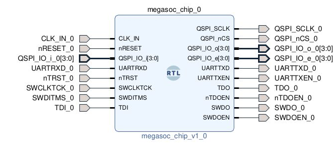
FPGA implementation utilisation is as below:
- LUTS: 307739
- FF: 74275
- BRAM: 36
- DSP: 8
- LUTRAM: 75753
There is still some optimisation to do in terms of the FPGA, timing currently only passes at 5 MHz using an external clock, plans for megaSoC will be to introduce a PLL and hopefully this can be increased. There are also some hold time issues that need to be looked into, this is probably related to the very simple constraints that are currently set (only external constraints at the moment, i.e. clocks and IO).
Connecting to Debugger
Using the ARM MPS3 and ARM D-Stream debugger we are able to successfully read the ROM table over the SWD and JTAG interface. With the APB ROM table as bellow
- ROM table base 0x40000000
- Coresight Base address 0x4001000
- CTI Base address 0x40020000
Cortex A53 is successfully detected. So for now the DAP-lite integration is successfully validated
Next Steps
Although there is still some more work to fully verify this CPU subsystem, it is now time to move this into a larger SoC infrastructure. This development will be continued in the MegaSoC project as we add more of the wider SoC architecture.
Project Milestones
Do you want to view information on how to complete the work stage ""
or update the work stage for this project?
-
Minimum bootable system
Target DateCompleted DateBuild minimum capable system and boot compiled software. Including Cortex A53, SRAM, UART, and XiP QSPI
-
Fix issues with QSPI
Target DateCompleted DateFix QSPI issues now that system successfully boots
-
FPGA SoC Prototyping design flows
Design FlowTarget DateCompleted DatePrototype the CPU subsystem in FPGA
-
Getting Started
Design FlowTarget DateCompleted DateFollowing the guidance for the Getting Started milestone to set up the project:
Project Management:
This project will follow the normal path of design flow steps. As the project is to be a foundation for the megaSoC reference design it may not go through to Tape Out and silicon validation. Additional free form milestones will be used to meet target dates to better drive the project to completion. As milestones are completed the date and details of the work will be captured.
Design Method:
The project will use an agile method, with short development cycles. Agile usually defines a first iteration as a Minimal Viable Product. In this case we define a 'Minimum bootable subsystem'.
Access to IP:
The IP required for this project is listed on the right hand panel of this page.
Version Control:
This project held in the SoC Labs git repository. SoCLabs / MegaSoC Project · GitLab
Project Structure:
See above project.
Verification Methodology:
This project will follow a typical SoC Labs reference design flow deployment using the SoC Labs continuous integration / deployment environment.
Team
Initial Prototype Project for:


 Daniel Newbrook
 Cortex-A53
 CoreLink NIC-400
 Corelink DMA-350
 SPI/QSPI
 GIC-400 General Interrupt Controller
Comments
Can't generate the DMA-350; address_map_m1_megasoc.sv is missing
Hello,
I am trying to run the example project; however, when I tried to generate the IPs, I got this errror massages from the DMA:
It seems that the address_map_m1_megasoc.sv is missing in the source tree.
Would you please help to solve this issue?
Thank you very much.
Fix in latest Git repo - megasoc_project
Hi,
Thanks for getting in contact about this issue. I'd forgotten to add the address_map_m1_megasoc.sv file to the repository.
The newest update should work now. Just as a warning, this project is still under development so there may be some major changes happening. If you do find any bugs like this please let me know and I'll try to resolve them as soon as possible.
Daniel
Directory 'expansion_subsystem_tech' missing
Hi Daniel,
Thank you very much for the quick response.
I still got an error because the
expansion_subsystem_techdirectory is missing.This is the output of 'make compile' command:
I tried to change the variable
SOCLABS_MEGASOC_EXP_TECH_DIRinto$SOCLABS_PROJECT_DIR/megasoc_techby modifying the makefilebut some files are still missing:
In addition, the variable '
CORTEX_A53_IP_LOGICAL_DIR' is set to/research/AAA/ip_library/Cortex-A53/MP030-r0p4-52rel2/MP030-BU-50000-r0p4-52rel2/cortexa53/logicalby default. I think it is better to set it to '$(ARM_IP_LIBRARY_PATH)/Cortex-A53/MP030-r0p4-52rel2/MP030-BU-50000-r0p4-52rel2/cortexa53/logical' which can be customized based on the ARM_IP_LIBRARY_PATH.Duy Hieu
Expansion Subsystem tech
Hi Duy Hieu,
The Expansion subsystem is a seperate git submodule. It may the case that this was added more recently. This link may help: https://stackoverflow.com/questions/1030169/pull-latest-changes-for-all-git-submodules
You will also have to run 'make first_time_setup' from the expansion_subsystem_tech directory. I will try to make this easier to do in the next update
And thank you for that suggestion, I will implement that change in the next update
Daniel.
Currently this is not working
Daniel,
Thanks for the update this week on the a53 project. I think it is refreshing for everyone to see that it is not always easy going getting these early stages in place and also that while arm IP may be 'Pre-verified' there are always some issues to overcome.
John.
Hi David and Daniel. Let me…
Hi David and Daniel. Let me know if I can pitch in and help with anything.
Add new comment
To post a comment on this article, please log in to your account. New users can create an account.