AXI Chiplet Controller
For a chiplet system, you need a communication interface between chiplets. The industry has developed standards that require complicated IPs around UCIe and the CHI interface from Arm. For many academic projects these are probably more complicated than needed . The aim of this project is to produce a simple chiplet communications interface based around the open standard AXI protocol.
The project is hosted here: https://git.soton.ac.uk/soclabs/chiplets/axi-chiplet-controller
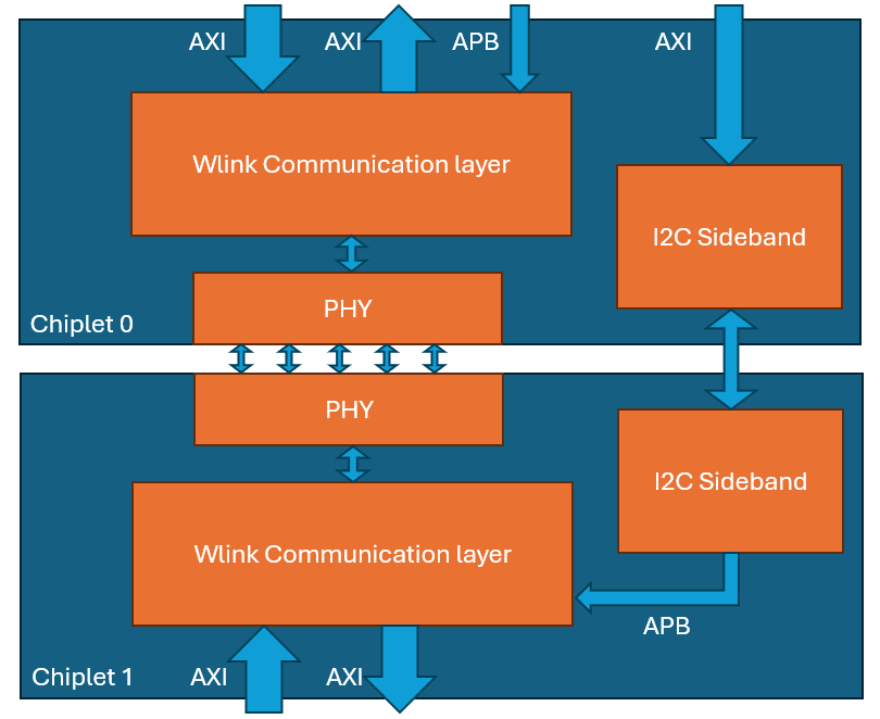
This project will build up prior work on wlink made available from wavious. The company was focused on developing a chiplet ecosystem, but looks to no longer exist in terms of support. An open source repository is available of the Wlink IP, a low latency, packet based architecture for communicating between chiplets. This IP includes multi-lane support, parameterisable application protocols, power states, ECC/CRC error checking, and configurable link settings.
The project is no longer in active development. The repository contents have been copied into the axi-chiplet-controller repository to continue work on developing this IP for the SoC Labs community.
Chiplet Roadmap
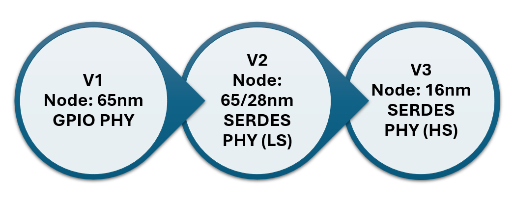
We have decided to separate this project into multiple milestones. The first of which is to focus on the digital design of the chiplet controller using as simple as possible PHY. This phase will use basic muxing and GPIO for the PHY drivers. This will give a baseline single data rate (SDR) communication interface, with limited clock rate of ~100MHz. Speed is not the target for this initial tapeout, the aim is to demonstrate baseline chiplet communication works, and that we can control multiple chiplets simultaneously.
Some work on Serdes PHY
A version using some previous developments before we had decided to tape out version 1 with a GPIO phy. The plan is to pick this work back up after we have done the initial V1 tapeout.
- PHY Development
For the second iteration of the chiplet controller, we are targetting a TSMC 65nm tapeout. We have chosen this to keep the PHY development as simple as possible. The specs for the PHY are as follows:
- Per lane bandwidth of 6Gbps
- Minimal area with most in the pad ring
- Pad pitch of 26 um
The biggest restriction here really is the area. And this will be the most important one for development of the PHY.
PLL
The purpose of the PLL is to provide a local clock for the chiplet PHY, and to provide a forwarding clock over the interface (Tx clock). For a 6Gbps bandwidth, we need a clock speed of at least 3 GHz. We also need to ensure the noise and/or jitter of this is as low as possible to keep transaction data as clean as possible.
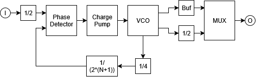
Why is there a divide by 4? The N-fractional circuit was having some trouble keeping up with high-frequency. I'm sure I can go back and figure this out at some point but for now this was the easiest fix to keep the input of the divider circuit as low as possible.
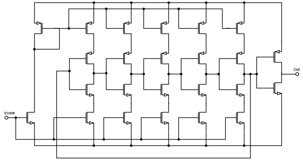
VCO
To keep area as low as possible, we are using a current-starved ring oscillator for this implementation (similar to https://soclabs.org/project/basic-pll-tsmc-65nm ). This implementation has a 5-stage ring oscillator with output buffer
The maximum frequency of this oscillator is about 7.5 GHz. Whilst this is more than needed for the application, it also means we can divide the output by 2 (possibly giving a cleaner clock) to get towards our 3 GHz. It also allows for the possibility if we are able to increase the bandwidth of the trasmitters/recievers and still use the same VCO circuit.
PLL Performance
For an input divider ratio of 3 (which should give an upscaling of 4*2*(3+1) = 32) and input clock of 240 MHz (divided down to 120 MHz) We get the following performance after allowing the circuitry to settle.
- Output Frequency: 3.84 GHz
- Rise Time: 45ps +/- 1.25ps
- Fall Time: 38.5ps +/- 2ps
- Period jitter: 1.44ps
- Frequency jitter: 23 MHz
V1 - TSMC 65nm - GPIO PHY
The plan for 2026 is to tape out a design using a GPIO phy. This will use the standard GPIO cells from the TSMC library without any sort of DDR serdes or retiming. Effectively the aim of this is to test the protocol layer of the chiplet controller, we aren't expecting to get very high bandwidth data transfer between chiplets, but that is not the focus.
Aims:
- Prove the controller protocol layer in silicon
- Develop initial flows for chiplet design and integration
- Tapeout 2 chiplets - 1 host and 1 ethernet controller
Plan
The chiplet communication system will be exercised by the nanoSoC reference design for the system behaviour, as this is already silicon proven reducing the overall uncertainty of the project.
We are editing the nanoSoC system to accommodate 2 chiplet interfaces either side of the die on the host chiplet. And a single chiplet interface on the ethernet die.
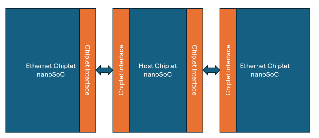
The final demo system will have 2 ethernet chiplets and a single host chiplet. The demo idea is to then run some sort of encryption/decryption engine on the host chiplet, and use the ethernet chiplets to communicate. This will demonstrate the use of the chiplet interface IP in a full system.
The details of the chiplets can be found in their respective projects (add links once pages are live)
- Ethernet Chiplet
- nanoSoC host Chiplet
AXI Chiplet Controller IP Design
The design of this IP is mainly a direct fork of the original wlink IP. With the addition of the I2C sideband, and some cleaning up of the APB address map to make it easier to control in software. Some further edits to this are currently being planned but for the initial IP design this is complete.
IP Verification
Initial verification has been complete using a cocoTB testbench of the IP. A full verification plan is currently being developed.
IO Floorplanning
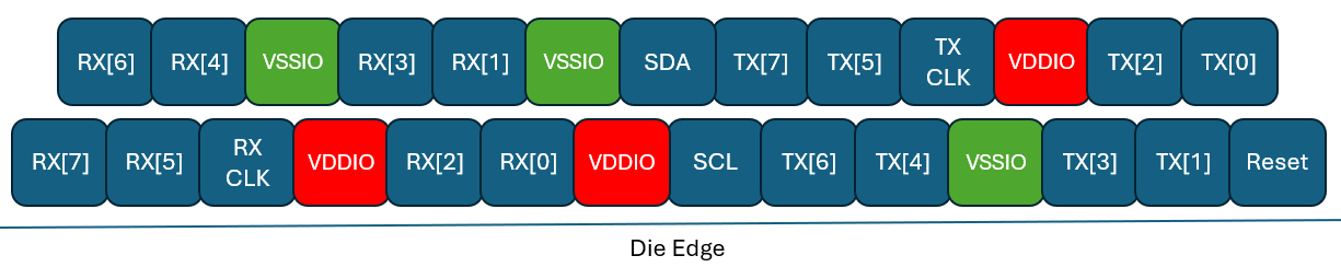
For the first iteration of this project, we are going to wirebond 2 dies together onto a PCB. The die-to-die connections will be done directly by wirebonding, and then any off chip pads will be wirebonded onto the PCB.
The layout for the IO's is as below with the opposite edge of the die floorplanned as a rotation of this (to allow for the same ethernet chiplet to be connected on both edges)
Project Milestones
Do you want to view information on how to complete the work stage ""
or update the work stage for this project?
-
Behavioural Design
Design FlowTarget DateCompleted DateFull behavioural design of the digital components in this system
-
Tape Out
Design FlowTarget Date

 Daniel Newbrook
Digital Design Engineer
at University of Southampton
Research area: IoT Devices
ORCID Profile
 Wired Off-Chip Communications
Submitted on
Comments
Relating this to other SoC Labs and broader industry activities
There are a number of other SoC Labs projects that are looking at the Chiplet implementation space and these are a very small subset of the broader activities in this area. It would be useful to be clear where this work fits into the overall design space for Chiplet based systems.
The first project in SoC Labs was the SRAM Chiplet. It explores the use of Arm IP to create a memory chiplet design. The Arm Thin links (TLX-400) was the IP investigated for the inter-chiplet exchange. This allows full AXI or AHB protocols to be converted it into an AXI stream interface for transmission between chiplets.
This non-Arm IP based project clearly offers some alternate method to enable inter-chiplet communication. Understanding the relative benefits/trade offs would be beneficial.
Add new comment
To post a comment on this article, please log in to your account. New users can create an account.