megaSoC
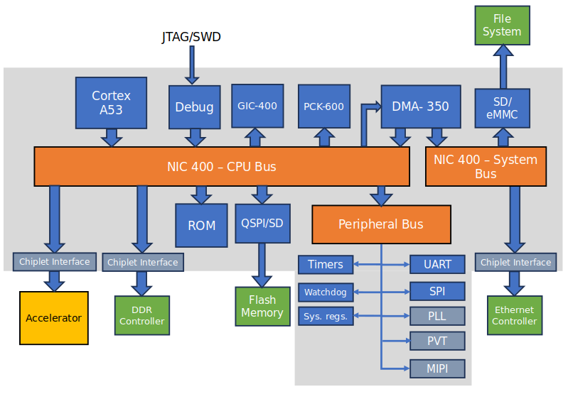
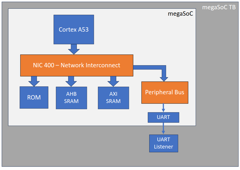
megaSoC is a high end reference design within SoC Labs. It provides a high performance System on Chip (SoC) using the Arm Cortex A53, that can be extended for design and evaluation of research blocks or subsystems. megaSoC is loosely based on the Arm Corstone 1000 subsystem, but with a simplified architecture to reduce tape out costs (no big.Little architecture, no security features, single processor/cluster design). megaSoC has been designed to be a reusable SoC design that can add memory-mapped experimental hardware, while simplifying the SoC design process with seamless transition from FPGA prototyping to physical silicon fabrication and evaluation.
To reduce the costs associated with academic routes to tape out, megaSoC is designed as a chiplet based subsystem. The main SoC will be an independent chiplet with research project accelerator subsystems on separate chiplets. This means that the central megaSoC chiplet can be taped out once, giving 100 separate dies that can be used on 100 separate projects. This makes the complex A class SoC systems a one time upfront cost, the ongoing cost of multiple projects will be greatly reduced. It will improve efficient use of silicon, as the same processor etc. will not require fabrication every time you make a new custom hardware SoC.
megaSoC is ideal for an academic team to evaluate research hardware in a SoC that can provide significant CPU performance, such as high speed pre/post processing data, and/or complex software stacks such as a Linux operating system. megaSoC is still under development and we welcome collaboration.
Reference Design Comparison Table
This table will let you compare this reference design with others on SoC Labs| Title | nanoSoC | milliSoC | megaSoC |
|---|---|---|---|
| Class | Entry | Mid Range | High End |
| Reference Design | nanoSoC | milliSoC | megaSoC/Corstone 1000 |
| Staffing | Single student / academic | Academic + dedicated post-doc | Academic Team |
| Time Scales | 6 months to 1 year | 1+ years | 18 Months - 3 Years |
| Model Forms | small | Real Time | Full Video/Large AI Model |
| Tape Out / Package and Board Costs | From 10k Euro | 25k-50k EUR | >50K - >>50K |
| Processor(s) | M0 | R5 | A53 |
| Processor(s) (speed) | <250 Mhz | 250-800 MHz | 1 GHz |
| Data Rates / On Chip Comms | <2.5 Gbps | 10-80 Gbps | >100 Gbps |
| Data Rates / Off Chip Comms | <50 Mbps | 0.1 - 0.8 Gbps | >1 Gbps |
| On Chip Memory Requirements | 32KB to sub MB | 2 MB+ | 4 MB+ |
| Virtual Prototype Environment | Xilinx ZCU104 | Arm MPS3 | HAPS |
| Tape Out Node | 65nm | 28nm | 16nm |
Related Projects and Workflows
This section details the following: the core reference design, the initial project that led to the definition of the reference design, and any additional projects that extend the reference design for new or additional applications. It also defines the related example workflows for the front end Architectural and Behavioural design stages, and the back end Logical and Physical design stages. Front end Behavioural design are usually accomplished with FPGA environments and tool chains, back end Physical design requires technology specific design rules and EDA tool suites.


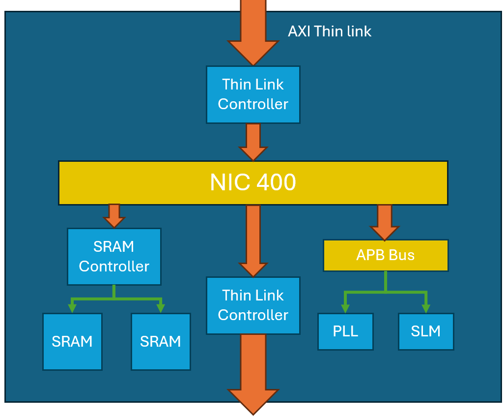
On-chip SRAM in ASICs can use a significant area, which equates to a significant cost. One solution is to make the memory off-chip. This project explores the use of Arm IP to create an SRAM chiplet design. The benefit is that standard memory chiplets can be fabricated at lower cost and used across multiple projects, miminising silicon area to the unique project needs.


 Daniel Newbrook
Add new comment
To post a comment on this article, please log in to your account. New users can create an account.