Enhancing HLS4ML: Accelerating DNNs on FPGA and ASIC for Scientific Computing
Project Motivation and Goals
Efficiency in hardware is vital as neural network models become more complex to tackle challenging problems, and optimizing ML hardware architectures has become a crucial research area. Scientists around the world, such as particle physicists at CERN need to accelerate their ML models in FPGA or custom ASICs for various applications including compressing the gigantic amount of data generated by the detectors at Large Hadron Collider (LHC).
However, implementing a DNN in hardware involves painstaking RTL design & verification, which takes time and effort. To solve this problem, HLS4ML, a user-friendly Python library was developed at CERN, enabling physicists to program ML code in Python and build synthesizable hardware on an FPGA through HLS (high-level synthesis). It is widely being adopted in the scientific community.
Yet, HLS4ML has limitations, particularly in supporting large-scale deep neural networks (DNN), which are crucial for many applications. Our project aims to address this limitation by creating a backend framework supporting large-scale DNN networks. This will enable efficient implementation of optimized hardware architectures on FPGA and ASIC for modern applications.
To be more specific, HLS4ML currently infers a new hardware module for each layer of the DNN in FPGA, making resource consumption scales quickly with the depth of the network. As a result, it is not possible to implement anything like a ResNet using HLS4ML. Thus, in real applications, it is desirable to process multiple layers in a single hardware engine. Our project seeks to make these hardware modules reusable, i.e., enabling data to flow through the same engine for multiple times, representing multiple layers. Therefore, we can allow the construction of large, complex ML models with limited hardware resources for various applications.
Workflow of Our system:
- One or more Qkeras models are first converted into an intermediate representation: a chain of Bundles. Each bundle is a group of layers such as Conv2D/Dense, Maxpool, Activation, Quantization, and Residual Add.
- The number of ROWS & COLS of processing elements can be freely chosen to fit a given FPGA or to meet certain area of silicon.
- The bundles are analyzed, and a set of synthesis parameters are generated. These are saved as .svh, .tcl, and .h headers. Controller code (C / Python) is generated for each model
- The project is synthesized, placed, and routed using given TCL scripts for those synthesis parameters using Cadence tools (ASIC) or Xilinx Vivado (FPGA)
- Randomized Verification: Our test suite generates random inputs, builds test vectors, and invokes a simulator: xsim, Icarus Verilog or Xcelium, randomly toggling bus signals to ensure correct behavior. The output vector is compared with the expected vector.
- Gale level verification is done using same test suit
- Realization (ASIC tape out steps or FPGA programming steps)
- Controller code is programmed into the chip and tested
Accelerator Architecture
Innovation
While there are several hardware accelerators available, they are either tailored for particular neural networks or have their own difficult-to-use workflows. We integrate our design into HLS4ML, hence solving a major problem in a tool widely being used in the scientific community. In addition, our architecture has the following features:
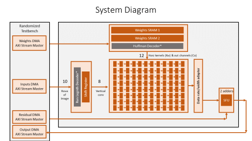
- Uniform dataflow: Conv2d, Dense, and Matmul layers are all executed through similar dataflow, with 100% PE utilization
- AXI Stream Design: Each module is built with AXI Stream interfaces, therefore can be easily implemented into various SoC architectures
- Distributed controller: A header of a few configuration bits is sent along the datapath itself, which is received at various stages of the pipelined design to reconfigure those stages locally, on-the-fly within one clock. This eliminates the need to flush the entire pipeline to process a different layer or a new DNN with a different size. PEs dynamically regroup to process different kernel sizes optimally.
- PE-Design: A processing element here consists of only a multiplier, adder and pipeline registers. Partial sums are kept only inside accumulators through the entire processing, to produce an output pixel. No SRAMs are needed to store partial sums.
Project Repository & Structure
Our source code is maintained as open source here: https://github.com/abarajithan11/dnn-engine
- asic - contains the ASIC workflow
- scripts
- work
- pdk
- reports
- outputs
- fpga - contains the FPGA flow
- scripts
- projects
- rtl - contains the systemverilog design of the accelerator
- test
- py - python files to parse the model, build bundles, and the pytest module for parametrized testing
- sv - randomized testbenches (systemverilog)
- vectors - generated test vectors
- waveforms - generated waveforms
Project Milestones
Do you want to view information on how to complete the work stage ""
or update the work stage for this project?
-
1. RTL Design of Accelerator and Verification
Target DateCompleted Date -
2. Developing ASIC flow (65 nm GP) and FPGA flows
Target DateCompleted Date -
3. RTL + Testbench auto verification using CI/CD Github Actions
Target DateCompleted Date -
4. Software: Qkeras based bundle, verifying fixed point operations
Target DateCompleted Date -
5. Software (bundle) + RTL flow tested on FPGA for an entire CNN
Target DateCompleted Date -
6. C firmware + RTL + Bundle on FPGA & 65m LP ASIC flow
Target Date
Team


 Project Creator
 Abarajithan Gnaneswaran
PhD Student
at University of California, San Diego
Research area: VLSI, FPGA, ML
ORCID Profile
Submitted on
Comments
Reviewing the project
The nice thing about this project is that is looking to "Empower Scientific Edge Computing", trying to simply via abstraction the effort needed by the broader science community, such as physicists and other scientific disciplines (beyond our core computer engineering community), to deploy Neural Networks.
Like all good science it builds on prior work, in this case the HLS4ML open source python framework. HLS4ML utilises high level synthesis (HLS) to take machine learning models and translate them to run on FPGAs. Scientists can rapidly prototype models in familiar environments and then use the available backend tool chains for implementation.
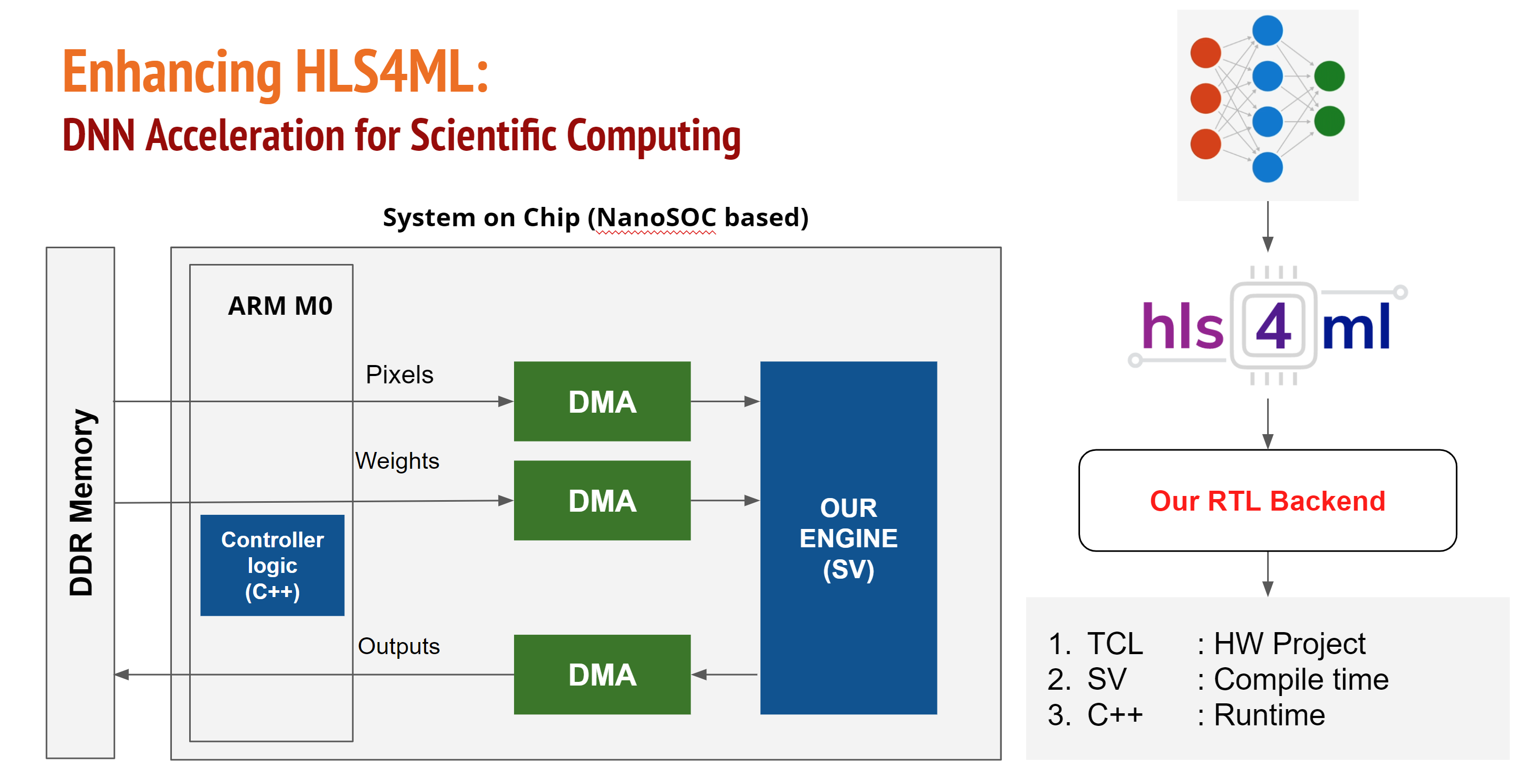
The CGAR4ML project also provide an abstraction layer in the design workflow and specific IP to allow more efficient deployment of models on FPGA and ASIC as a custom accelerator.
The challenge in this project has been the integration of a target reference design for a SoC implementation into the ASIC target while maintaining the alternate FPGA target. The Xilinx Vivado FPGA target uses an AXI interface with a number of DMA channels to move data into the custom accelerator engine.
The nanosoc reference design is a simple M0 microcontroller based system for supporting research hardware such as a custom accelerators with an easy transition from FPGA to physical silicon ASIC. As an M0 based design it uses a simplified AMBA AHB bus design. The challenge then is to select appropriate IP blocks to bridge between the nanosoc design and the AXI based CGAR4ML custom accelerator.
Bridging between nanosoc and the CGAR4ML custom accelerator
The advantage to the research community of nanosoc reference design is the target design rational of a simple design that academics can understand and a low cost of implementation. The projects that have progressed through to tape out and demonstration using the low cost test board are;
Fast-kNN: A hardware implementation of a k-Nearest-Neighbours classifier for accelerated inference by Epifanios Baikas uses the DMA 230 for data transfer into the custom accelerator.
The concept for this project was to attempt to also use the DMA 350 for data transfer into the CGAR4ML custom accelerator. The added design challenge being to maintain close compatibility with as much of the alternate FPGA IP.
The initial nanosoc design had optional support for 1 or 2 Direct Memory Address controllers and two banks of DMA-accessible SRAM buffer space for concurrent expansion space for use by custom accelerators. To accommodate the CGAR4ML custom accelerator additional DMA channels are required and AHB / AXI interfacing. There are also considerations on how the use of interrupt handling for the DMA 350 on the M0 processor would operate compared to the firmware model within the CGAR4ML environment used to control the custom accelerator.
NanoSoC integration
We have developed an over-arching project structure for integration with the NanoSoC. You can find the repository here as well as an example project integrating a AES128 accelerator
In order to use this structure, you will have to fork the "Accelerator Project" repository, and then either clone in your accelerator repository, or add this as a submodule (instructions for this are in the readme). Once you have done this you will have to edit a couple of files. ./env/dependency_env.sh should be edited to add your accelerator directory, and the files in flist/project will need to be updated to add in the files of your repository.
When you have cloned this project structure you should run "source set_env.sh" This will allow you to use the socsim environment. This can be used to run simulation scripts from the simulate/socsim directory.
We are currently updating the documentation but hopefully this is enough to get you started
Establishment of SoC Labs Project structure
Thanks for the great description of the project. I quick look suggests integration of NanoSoC MO and DMA controllers with your project. I hope I have not mis-represented this. Look forward to seeing the Project structure to bring in the various parts and the design flow environment for the project.
Add new comment
To post a comment on this article, please log in to your account. New users can create an account.