DMA Infrastructure Developments
Project Aims
SoC Labs aims to produce reusable SoC reference designs using the variety of AMBA bus architectures.
Project Status
An initial NanoSoC reference design using AHB for small scale accelerators with low data throughput and complexity is complete. This design has had two projects tape out with proven silicon implementation of two DMA Infrastructures with ASICs operational in the same test board:
Fast-kNN: A hardware implementation of a k-Nearest-Neighbours classifier for accelerated inference uses the low gate, DMA 230 and was implemented by Epifanios Baikas
Hell Fire SoC uses a higher throughput, DMA 350 and was implemented by Srimanth Tenneti
The project is now working on further collaborations on AXI based SOC, for larger scale accelerators with higher data throughput and added complexity. It is also developing an alternative light weight DMA infrastructure for an additional NanoSoC based design.
Why do we need a DMAC?
In a SoC with a data-hungry accelerator, there will be a lot of data to move around the system. To perform this using a CPU is inefficient, means the CPU is often busy and cannot be used for other purposes, such as more important data processing or system analysis actions.
One way to get around this problem is to have a dedicated Direct Memory Access Controller (DMAC) which is responsible for moving data around the system, especially moving data between the on-chip RAM and any custom hardware accelerator.
The following criteria are some of the design decisions that need to be made that will affect the bus implementation strategy and the DMAC controller used:
- System Bandwidth - How much data is going to be moving around are SoC?
- Ease of adoption - How quickly and easily can someone use the DMAC in their design and test methodology?
- Footprint - What are the physical design implications of the decision choices?
What bus protocol should be chosen?
Arm have produced an open-access collection of bus architectures called AMBA (Advanced Microcontroller Bus Architecture) which contains three main interconnect specifications: AXI, AHB and APB.
AXI is more suitable for higher performance SoCs offering higher bandwidth but has a larger design overhead, increased footprint and increased complexity compared to AHB and APB.
Below are outlines for two SoC implementations:
- AHB based, for smaller scale accelerator prototypes with lower data throughput demands and less complexity
- AXI based, for larger scale accelerator prototypes with higher data throughput demands but added complexity
- AHB based NanoSoC - Project Status: Completed
1 - Interconnect Implementation
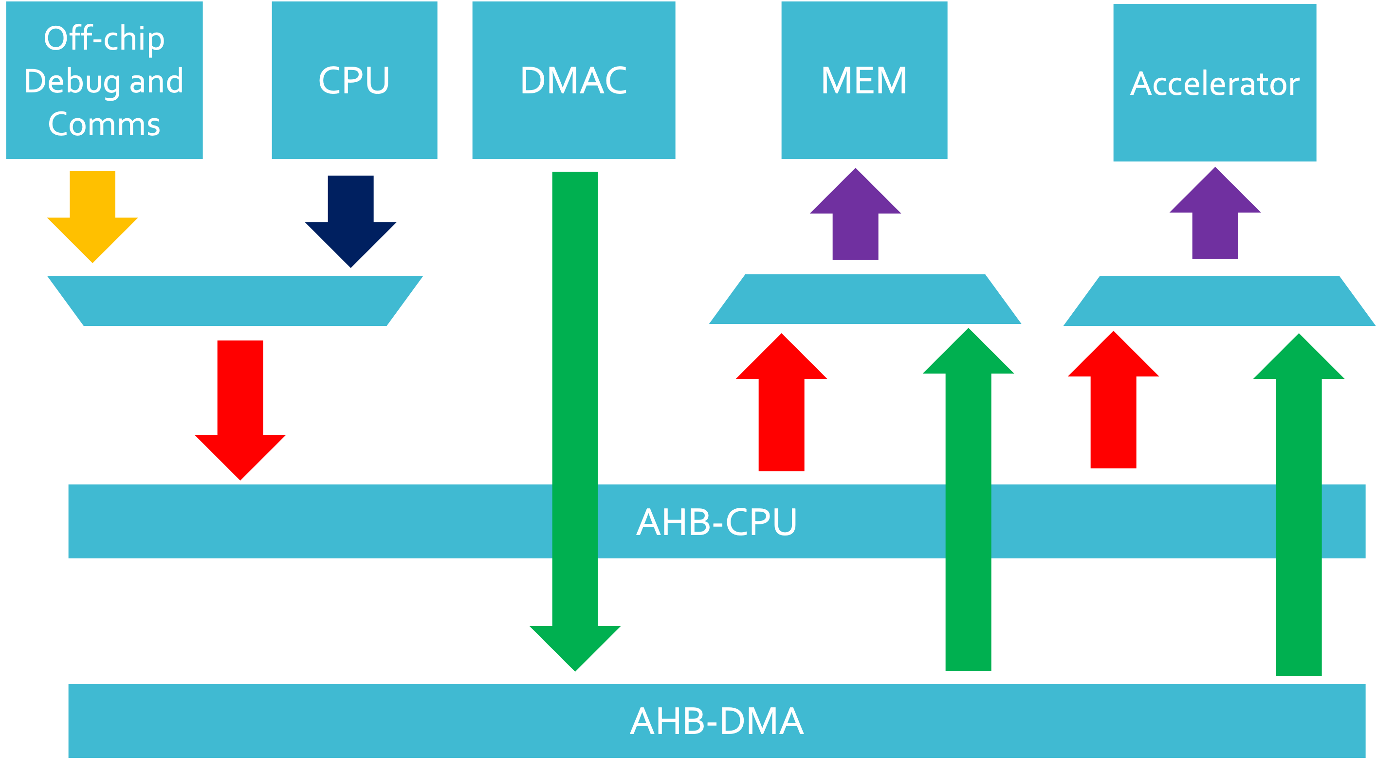
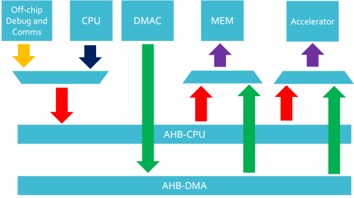
APB is designed for peripheral devices with low bandwidth which is non-pipelined and doesn't support multiple initiators or burst transaction - these are all features AHB supports. Because of this, AHB has been selected for our primary interconnect.
With the AHB-based SoC infrastructure that we will be using, a DMAC could cause high levels of congestion on our buses so to get around this, we have the following options:
- Multiplex AHB Initiators onto the AHB bus
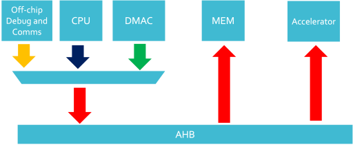
- Run a parallel AHB bus and the multiplex off of the buses to the desired targets.
For more information on the configuration of the bus interconnect implementation please see our case study: Building system-optimised AMBA interconnect
2 - DMAC Selection
So far, an obvious contender for the DMAC we will be putting in this SoC infrastructure is the Arm DMA-230 also known as the PL230.
The advantages of the PL230 are:
- Low gate count
- Simple to understand
- Multiple channel support
- documentation available
- Verification IP available
The main disadvantages of the PL230 are:
- Quite inefficient - lots of additional reads and write to update transfer progress to memory - no internal memory
- Quite limited on it AHB setup - a lot of features available with AHB are unsupported
- The main feature that is missing is burst transfers which can be incredibly useful
3 - Data Availability
A large contributing factor to the implementation is related to the amount of data that is going to be moved around the SoC. It is going to be vital that any accelerator engine is going to have enough input data to process and output data is moved away from the accelerator fast enough to not stall the accelerator and ensure accelerators are able to push their performance.
The system AHB and APB buses have a limited amount of bandwidth which is determined by multiple factors including the the bus data width, bus congestion and bus clock speed. In cases where the bandwidth of data is insufficient compared to the required bandwidth of the accelerator, the accelerator will stall. To get around this, decisions can be made on both the accelerator wrapper and SoC infrastructure sides of the design.
System Infrastructure
Bus data widths - by increasing the data widths of the bus, more data can be moved per clock cycle.
Relative Clock Speeds - by having the bus (and other memory components) running at a faster speed compared to the accelerator, more data can be available at the accelerator per accelerator clock cycle.
DMAC Selection - back to part 2, having an efficient DMAC, more clock cycles can be spent transferring data to the accelerator.
Interconnect Implementation - in addition to section 1, having multiple DMA buses and multiple DMAC's, more data could be transferred to an accelerator per clock cycle, concurrently with the system control microprocessor.
Some of these choices are easier to implement than others but each design choice has considerations of the physical implementation, user data management and system configuration in software.
Accelerator Wrapper Infrastructure
A generic solution for this Project would be ideal if it had no need to impose any major design restrictions or changes to custom accelerator IP. Any practical changes to accommodate the system bandwidth should be made in a wrapper around the accelerator engine.
Data reuse - by considering that data that is being processed and the order of the data being processed, some data could be buffered and used in multiple accelerator operations. Building a buffer and only replacing some of the data reduces the amount of data that needs to be transferred into the accelerator.
Configuration Registers - by including a few registers in the wrapper, configuration inputs to accelerators can be stored for cases where the configuration may remain constant over multiple operations.
By breaking the wrapper into two sections - one for handling the accelerator interface to the AHB and APB buses and an intermediate one including control, status and buffering logic could provide a solution or a part of a solution to the data availability problem.
Project outcome
This project has now been completed, code/RTL for the SoC infrastructure can be found on GitLab
If you are interested in using this SoC infrastructure for your accelerator, we have also developed a project structure which you can fork for your own projects (found here)
- AXI based SoC - Project Status: Call for collaboration
1 - Interconnect Implementation
ARM provides two categories of bus architecture for an AXI implementation: Cache coherent interconnect (CCI) and network interconnect/non-coherent (NIC). Cache coherency allows for "operating systems to be run over multiple processor clusters without complicated cache maintenance software". This allows for ARM's big.LITTLE processing model, as well as having coherency between a CPU and accelerator. To allow cache coherency ARM has extended it's AXI bus protocol to the ACE protocol, which included functionality to enable it's cache coherency.
2 - DMAC Selection
An obvious choice from ARM would be the DMA-350. This has many benefits over the PL230:
- 32 - 128 bit data width
- 32 - 64 bit address width
- 1 or 2 AXI5 master interfaces
- Extended feature set: 2D copy, templates
- AXI stream interface
- Higher transfer efficiency
However, the cost of this is increased complexity and gate count.
3 - DMA-350 Verification environment
To develop a verifcation environment a SoC subsystem has been created to explore the functionality of the DMA and verify this functionality. The verification is done using cocoTB with Mentor Graphics Questasim, although this could be used with any simulator. The repository for this can be found here.
The SoC subsytem is shown below, comprising of the DMA-350, NIC-400, BP140 (AXI memory interface) and a pipelined FIFO:
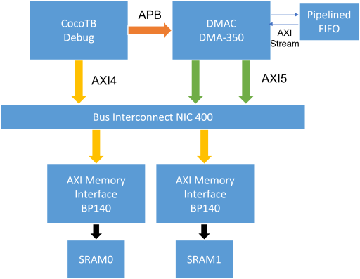
The 3 master interface of the NIC400 are: 2 for DMA-350 and 1 for debug access. The debug access could be replaced with a CPU or debug controller.
The address map for the SRAMs are:
Base Address End Address Size SRAM0 0x00000000 0x00004000 16KB 0x08000000 0x08004000 16KB SRAM1 0x10000000 0x10004000 16KB 0x18000000 0x18004000 16KB The 2 alias address at 0x08000000 and 0x18000000 are used so that the DMA-350 can access the same data space through both of the AXI masters. When configuring the DMA 350 you have to give a mapping for the AXI Master 1, in this case if addr[27] is high then AXI Master 1 is used, otherwise AXI Master 0 is used.
CocoTB Verification
SRAM:
To begin verification of the subsystem, 3 test cases have been developed. The first is to test the writing and reading from SRAM0 and SRAM1 at both of the available base addresses. This testcase was based off Alex Forencich's cocoTB AXI tests which writes data at address offsets of 0-8 and 7F8 - 7FF (first 8 and last 8) with burst lengths of 0 - 15 and 1024. Once a write has been performed, a read is then performed at the same address and length and asserted equal. If these aren't equal then the test fails.
DMA AXI interface:
A simple 1D transfer test is then performed. To achieve this, first random data is written to SRAM0. Next the APB channel is used to program the internal registers of the DMA-350. The minimum required setup is: Source address, destination address, source and destination size, configuration bits, source and destination transfer configuration and address increment.
Once set, the ENABLECMD bit can be set high to start the DMA.
When the ENABLECMD bit is set, we also start a timer, this is then used to calculate the effective data bandwidth of the subsystem. Which for a clock frequency of 1 GHz is 43 Gbps.
Verification of the test is done by reading from SRAM0 and SRAM1 and comparing values to see if the write was performed as expected.
DMA AXI stream interface:
A similar test for the axi stream interface is also performed. The DMA axi stream is connected to a pipelined FIFO with parameterisable pipeline length. This is used to emulate a hardware accelerator that has some pipeline delay between input and output.
First random data is written to SRAM0 (at 0x00000100), then the DMA is setup with the stream interface. The difference in configuration is in the CH_CTRL register, which has the DONETYPE = 0, REGRELOADTYPE = 0, and USESTREAM = 1. CH_STREAMINTCFG is also set to 00 for stream in and out used. By using the stream interface with some pipelined hardware, we introduce some delay and therefore for a 1 GHz clock we have a total effective bandwidth of 36.9 Gbps. The bandwidth is calculated using the time between the start and end of the DMA.
Project outcome
This project has now been completed, code/RTL for the DMA-NIC subsystem can be found on GitLab
Request for collaboration
Team


 Daniel Newbrook
Digital Design Engineer
at University of Southampton
Research area: IoT Devices
ORCID Profile
 CoreLink DMA-230
![]() Hardware design
Hardware design
![]() Getting Started with SoC Labs
Getting Started with SoC Labs
![]() Architectural Design
Architectural Design
Submitted on
Comments
Any update?
Any update?
Uodate
Hi,
We have started work on a new DMA implementation. This will use the DMA35. We are also looking into AXI based implementations for a higher bandwidth SoC reference design. We will add some information shortly.
John.
Initial DMA 350 activity
Daniel,
Thanks for updating the project to split out the NanoSoC AHB implementation from the new AXI implementation. Can you expand a little on the early DMA 350 investigations.
John.
How i can send my request?
Hello David i would like to join on this project but the link dosen't working!
Status
This request for collaboration has turned into some explicit projects to develop the parts of the lightweight SoC Infrastructure that cab be used with minimal modifications to implement experimental hardware accelerator prototypes.
Not all experimental hardware accelerator can be supported by the current reference design. It would be good to get people to contribute additional SoC Infrastructure designs.
Sign up Link
Hey,
Is there a link where we should signup for the collaboration?
Thanks, & Regards
Srimanth Tenneti
Sign Up Link
Hi Srimanth,
Not just yet. I think by commenting on this article you should now get any updates for this page. I'll work with John to try and get a system sorted to make this easier in the future.
Thanks,
David Mapstone
Sign Up Link
Hi,
In the mean time, adding a comment worked and I have added you. Whatever works, if people express and interest we will make sure we note it. Looking forward to working with you on this.
John.
Sign up link in the Actions.
For projects we have now added a sign up link in the Actions.
Add new comment
To post a comment on this article, please log in to your account. New users can create an account.