Arrhythmia Analysis Accelerator : A-Cube
We propose the A-Cube design methodology to create medical decision support on the edge. The design and implementation of an atrial fibrillation detector hardware core was selected as a proof-of-concept study. To facilitate the required atrial fibrillation functionality, we adopted an established AI model, based on Long Short-Term Memory (LSTM) technology for hardware implementation. The adaptation was done by varying design parameters such as data window and the number of LSTM units. We found that a data window of 40 beats and 20 LSTM units are sufficient to achieve a classification accuracy of 99.02%. We are confident that the A-Cube methodology can be used to implement this model in hardware. Doing so, will create a low power and low latency atrial fibrillation monitoring solution which has the potential to extend the observation duration while being convenient for patients.
Physical Implementation
Technology selection
Some investigation was made between the trade-offs between using TSMC 65nm and 28nm technology nodes. To begin with a synthesis run for 65nm was completed and found the accelerator to be significantly larger than expected.
After this some tests were done using TSMC 28nm to compare the area, power, and cost of the dies. Showing that the reduction in core area leads to a more reasonable cost of the die, whilst also giving better power performance.
| TSMC 65nm LP | TSMC 28nm HPC+ | |
|---|---|---|
| Die Size | 2.2 x 2 mm | 1.5 x 1 mm |
| SRAM Memory | 64 KiB | 64 KiB |
| Accelerator Area (µm2) | 2,440,320 | 726,110 |
| Gate Count | 445,197 | 575,824 |
| Accelerator Power (mW) | 722 | 201 |
| Clock Speed (MHz) | 240 | 240 |
| Projected Cost | 13,541 | 10,777 |
Timing closure
Whilst investigating the use of TSMC 28nm libraries, this did introduce some violations in the timing closure. After a long time of investigating different possible causes, we finally figured out that the issue was the choice in standard cell libraries.
At 65nm, there were 3 track height options and 3 threshold voltage options. But for 28nm there were 3 track heights, 4 threshold voltages and 3 channel length options. Without really understanding the differences, we decided to use the 12-track S-VT and largest channel length. This would normally provide a fairly high performance design, as the drive strength of the cells would be quite high.
The problem however was in the balancing of setup timing and hold timing. The violations we had were in the hold timing, which requires longer delay paths to accomodate for. The EDA tools weren't able to insert enough delay for the hold timing to overcome the massive drive strength of the cells.
After some investigation we found that the 7-track S-VT library gave a good balance between the hold and setup timing. This also was the main reason for the large power reduction, as the drive strength of the cells is much lower.
Floorplanning
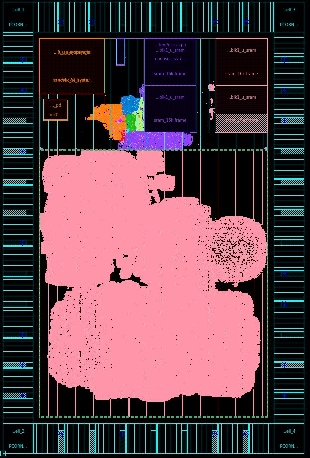
The floorplan for the die is shown as below. The bottom area (pink) is the A Cube design, with the top area being the core SoC of nanoSoC. There is currently quite a significant amount of 'spare' area. Partly this is whilst we are still developing the flow, and if we need to decrease cell density due to routing congestion (which is much more significant in the 7-track library), but also partly due to restriction in the cell height in mini ASICs. The height has to be a multiple of 0.5mm, and it was found that 1mm was too small, so 1.5mm was chosen.
Physical Verification
After spending a lot of time trying to figure out why timing wasn't working, and finally figuring it out, we'd hoped that then the implmentation would be 'nice and easy'. However, when trying to verify the gate level simulations, we ran into some issues. Initially, we found that the accelerator would output x's after being loaded with values and trying to run the calculations.
We managed to get past this issue by moving the HLS backend from using Vivado/Vitis, to using Siemens Catapult. This also seemed to give a much cleaner RTL for ASIC implementation. However this still gave x's from the output of the accelerator.
So we then tried running the synthesis directly in Catapult, and importing the netlist into the design. This way Catapult would hopefully setup all the constraints etc. correctly for the implementation of the accelerator. However, this gave new issues, it seemed after running gate level simulations that the data does not get properly captured by the accelerator from the system, so the accelerator then stalls.
It seems to be that either
- The synthesis process is breaking the accelerator somehow
- The boundary between nanoSoC and the accelerator is not working properly after synthesis
Currently we are trying to run different permutations in the Catapult synthesis, then in the full system design to get a clean result in the backend. But unfortunately the run time for Catapult is about 6-7 hours, and then synthesis of the full system is another 5-6 hours, and gate level simulations take a few hours to run and debug. This results in quite a lengthy debug cycle between stages.
Project Milestones
Do you want to view information on how to complete the work stage ""
or update the work stage for this project?
-
Getting Started
Design FlowTarget DateCompleted DateImplement and test the Soclab encryption example in the ZCU104 FPGA board.
-
Behavioural Modelling
Design FlowTarget DateCompleted DateImplement an atrial fibrillation detection model in the ZCU104 FPGA board.
-
data model
Design FlowTarget DateAnalyse the model performance based on different signal length and algorithm complexity.
-
data model
Design FlowTarget DateAnalyse the model performance based on different quantisation levels.
-
Behavioural Design
Design FlowTarget DateSelect a suitable implementation candidate to server as atrial fibrillation detection core.
-
Behavioural Modelling
Design FlowTarget DateCompleted DateSimulate (RTL) the selected atrial fibrillation detection core.
-
Generate RTL
Design FlowTarget DateImplement an AHB bus interface for the selected atrial fibrillation detection core.
-
Generate RTL
Design FlowTarget DateIntegrate Nanosoc and the selected atrial fibrillation detection core.
-
Simulation
Design FlowTarget DateCompleted DateSimulate the integration results.
-
RTL Verification
Design FlowTarget DateCompleted DateImplement the integration results in the ZCU104 FPGA board.
-
RTL Verification
Design FlowTarget DateTest the hardware on the ZCU104 FPGA board.
-
Technology Selection
Design FlowTarget DateCompleted DateExplore technology nodes for implementation
Result of WorkSynthesis comparison between TSMC 65nm and 28nm found that the cost/area would make more sense to run on 28nm as the core area was too large
-
Timing closure
Design FlowTarget DateCompleted DateResult of WorkNo timing violations in design
Team


 rami hariri
researcher student
at anglia ruskin university
Research area: AI
Submitted on
Comments
Generating the nanoSoC ASIC within HLS4ML
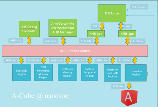
You are able to build nanoSoC with the DMA removed. The two nanoSoC designs taped out recently had either the DMA 230 or the DMA 350. Aba and the team are developing an accelerator core with micro DMA engines within their accelerator design. This allows them to generate similar firmware for their FPGA implementation as their ASIC implementation. They have been varying the nanoSoC project to build without the DMA 230 or DMA 350 IP but containing their addressing within the accelerator expansion region.
nanoSoC ASIC and HLS4ML
It would great if you could reference this new interest page on hls4ml in your project. It would also be helpful to get an update on milestones. Have you managed to progress Milestone 7?
Key moment in the project
Hi,
Can you please update us on the status of the key Milestones 7 and 8. Can you confirm you have at least got the base NanoSoC reference design integrated within your tool chain and expected work flow?
We look forward to hearing from you.
Key moment in the project
Hi,
Can you give an update as requested on the most recent milestones?
John.
milestone update
we have completed the bus interface and currently working on completing the FPGA verification by determining the correct location for the memory contents files.
milestone update
our current focus is on creating console output from the FPGA implementation which will determine how long the FPGA verification takes
Console Output
Hi,
Can you provide a little more detail, is this console output from the atrial fibrillation detection core or for the nanoSoC system. I think there is support for the later so it would be good to understand what is required.
milestone update
the console output from the FPGA implementation of the Atrial Fibrillation Detection core
Introduction
Atrial Fibrillation (AF) is a common heart rhythm disorder which increases the stroke risk fivefold . It is estimated that AF prevalence in the UK is around 1% of the general population and increases to 10% within the older population. AF is diagnosed by analysing the electrocardiogram (ECG) of the human heart. Figure 1 shows an ECG signal before and during an AF episode. This analysis can be done manually, which is labour intensive or with artificial intelligence (AI) models. Currently the AI models are executed in cloud servers and the data must travel from the point of measurement to that server over a network. Communicating the data requires network connectivity and energy expenditure associated with accessing the network. Furthermore, communication channels pose data safety and security issues. Moreover, a setup procedure is needed for transferring patient data to the cloud server. These systemic issues limit the observation duration of measurement equipment, such as patch sensors for heart rate capturing. The reduced observation duration will reduce the number of observable AF episodes which has a negative impact on AF diagnosis.
Architectural design pattern for data movement within the SoC
It was good to hear you confirm the Architectural design pattern for data movement within your proposed SoC. It was interesting talking through the various options:
Given the low data bandwidth requirements for you specific project you felt the DMA approach was not needed. A simple interrupt architectural design pattern with a mapping of registers within your custom hardware into the address space of the processor and accessible from the main system bus was I recall your proposed design. This will be a combination of data, status and result registers.
It will be good to see how this develops.
Planning for Design Under Test
Hi,
It was good to open the discussion on what will be your frame work for creating test benches. There are a variety of approaches people are adopting. The Verification pathway parallels the Design pathway through the Design Flow stages. There are even standarisation efforts in this area:
Universal Verification Methodology | SoC Labs
It often comes down to experience of various tools and languages that are easily adopted, or the ability to re-use prior verification assets that reduce the overall project timeline rather than extend it with new skills acquisition for unknown techniques.
There are some verification assets in SoC Labs and some projects to continue to develop these.
System Verification of NanoSoC | SoC Labs
I think you had some specific focused test bench requirements you wanted to work on for the data flow across the bus. I guess this is part of the usual ebb and flow of design, either top down for the SoC systems architecture or bottom up from foundation IP blocks.
Looking forward to seeing how these develop on your project.
John.
Progress to date
Hi,
It was great to hear today how you worked through the analysis to come to the view that the data window of 40 beats and 20 LSTM units are sufficient to achieve a classification accuracy of 99.02%. It was also interesting to explore how the data movement across the bus and into your accelerator will form based on this requirement.
Different people have taken similar but slightly varying approaches to how the data transactions flow into their working registers within their accelerators. There are a few projects that can act as examples:
SHA-2 Accelerator Engine | SoC Labs
Given the volume of data flowing I think you concluded the Master for the bus was likely the M class CPU and not a DMA controller.
All sounds very promising and it will be great to understand more on the design and expected milestones.
Interesting paper on FPGA implementations of ML
Here is an interesting paper on a model to determine FPGA resources for multi-layer neural networks. Part of their conclusions is “LSTM turned out to be very demanding on FPGA computing resources”. Do you have a view on the LSTM implementation you will need for this application?
Nanosoc Configuration
Hi Rami,
We've just updated the way you can configure nanosoc, to hopefully make it more easy for people to make changes to the overall configuration without having to change multiple files. If you pull the latest changes you should see a nanosoc.config in the nanosoc_tech directory
If you leave the options blank, they will not be included and if you write a yes (or really any text after) then it will be included. There is also a section to edit the paths to arm IP
You should now not have to make any edits to flists (apart from to include your accelerator) or to any of the makefiles
Let me know how it goes
Daniel
Updates to milestones (end of May 2024)
Hi,
It would be good to get an update on your milestones at the end of the month.
I think you have been working on the interface Atrial Fibrillation Detection Accelerator core to main Nanosoc. As I understand things, you were considering the need for a DMA for data transfer. If you do not use a DMA the processor will have to initiate all transfer of data between your sensor input and your custom accelerator.
Let us know where you have got to?
John.
Adding initial milestones
Hi,
Great to see the project live. It is very easy to add the initial milestones and you can come back as each milestone progresses and make updates.
IITH are a good example of milestones in their project https://soclabs.org/project/real-time-edge-ai-soc-high-speed-low-complexity-reconfigurable-scalable-architecture-deep
You can simply select milestones from the generic design flow stages or create any unique milestones.
Architectural Milestone
Hi,
How are you getting on with your work with the HLS4ML framework to find suitable deep learning models for your hardware implementation.
John.
Using HLS4ML as a modelling tool for Architectural design
The HLS4ML environment can use various backend tool chains for High Level Synthesis (HLS). These tools support the generation of variations of hardware implementation for an algorithm written in a high level language portable language. The benefit of High Level Synthesis is that it bridges hardware and software design domains.
It was good to get some details of your design environment. As I understand things you are using the Xilinx® Vivado® High-Level Synthesis (HLS) tool chain as your backend. HLS4ML uses streams to pass data and these are mapped into implementation buffers. As with other abstractions it provides an accelerated design environment but then requires effort to optimise the hardware implementation. This can be done by developing optimization directives that direct the tool chain to refine the automated generation of the implementation.
Alternatively some design teams move to use the next layer of tooling down in the design abstraction environment once they have a conceptual design. The data model for your project is relatively easy to understand. It was interesting discussing the use of the Xilinx® HLS streaming interface. We also discussed some of the challenges of moving beyond the FPGA fabric support into the full ASIC implementation flow and the subtle differences in performance of logic and memory between the two hardware instantiations.
It will good to hear how things are progressing.
Using HLS4ML to generate models
If you are still planning to use HLS4ML to generate a model you might be interested in one of last year's projects. I have added a few comments on what has been happening on Aba’s project by and the design challenges.
Enhancing HLS4ML: Accelerating DNNs on FPGA and ASIC for Scientific Computing | Review
Is my current overview of their project environment and
Enhancing HLS4ML: Accelerating DNNs on FPGA and ASIC for Scientific Computing | Bridge
Is an overview of the bridge issues from nanosoc to their custom accelerator
Translating HLS4ML models into ASIC implementation
The workflow proposed by Aba and the team in their project is developing but still has some issues being resolved to map the model to the nanoSoC reference design when dealing with the specifics of physical design for a specific technology node and ensuring there are no DRC violations. The section 'Workflow of Our system' is helpful in giving an overview. You should be able to get some understanding of the next milestones, I think these are 6,7,8.
One significant difference I am aware of is that the volume of data Aba and team are looking to move through the system is such they plan to use DMA engines to offload the data movement across the bus. In your case you have said the data volume is low and so you don't plan to use DMA. I am assuming the firmware on the M0 will handle the transfers?
Generating ASIC implementation from HLS4ML
In this interesting Siemens EDA presentation on Catapult + HLS4ML for Inference at the Edge it is clearly shown why generating the right intermediate code is important to allow efficient ASIC implementation.
David Burnette in this presentation illustrates a hardware design pattern, Sliding Window, and how generating the appropriate code from the HLS4ML environment allows the design pattern to be used to make an efficient implementation.
Data transfers and Firmware
Looking at this diagram from the ML Developers Guide for Cortex-M Processors and Ethos-U NPU your application is in the vibration detection class I suspect. As you are planning on using DMA then the M0 processor will handle the data movement through your custom accelerator.
Copyright © 1995-2024 Arm Limited (or its affiliates). All rights reserved
I recently updated the Interest on Firmware. I suspect you will need to develop a device driver for your custom accelerator to handle the interactions and interrupts.
A good example of milestones
Here is a good example of update to a milestone to add a completion date and show progress. It comes from one of last years projects.
It shows both the Completed Date and key additional information such as the reported area with a clear statement of the inputs that this is not using a specific technology node standard cells.
Update as of November
Hi,
It would be good to get some update on where we are with the milestones and also an update on the planned milestones that would take the project to an ASIC tape out?
We look forward to hearing from you.
Update as of end of November
Perhaps a Milestone 14 could be added? Now that Europractice have set out their schedule for 2025 fabrication shuttles then the 16th April mini@sic shuttle looks a good candidate for a nanoSoC version 2 tape out.
Is there a Milestone for the implementation of the Hyperbolic tangent and sigmoid functions ? When will this be complete?
Hi, you just need to save to…
Hi, you just need to save to Editorial and not Drafts to get it submitted. You can come back later and change.
Abstract
We propose the A-Cube design methodology to create medical decision support on the edge. The design and implementation of an atrial fibrillation detector hardware core was selected as a proof-of-concept study. To facilitate the required atrial fibrillation functionality, we adopted an established AI model, based on Long Short-Term Memory (LSTM) technology for hardware implementation. The adaptation was done by varying design parameters such as data window and the number of LSTM units. We found that a data window of 40 beats and 20 LSTM units are sufficient to achieve a classification accuracy of 99.02%. We are confident that the A-Cube methodology can be used to implement this model in hardware. Doing so, will create a low power and low latency atrial fibrillation monitoring solution which has the potential to extend the observation duration while being convenient for patients.
Add new comment
To post a comment on this article, please log in to your account. New users can create an account.