High Capacity Memory Subsystem Development
This project aims to design and implement a high capacity memory subsystem for Arm A series processor based SoC designs. The current focus of the project is the design and implementation of a Memory Controller for DDR4 memory.
Introduction
The efficient and cost effective use of memory is critical to SoC design. Significant design and intellectual property ("IP") blocks work in coordination within the SoC to deliver system level performance at a reasonable cost. Traditional SoC designs optimise memory use via a memory hierarchy. Within the processor, high speed registers are accessed directly by physical control signals for various compute actions. They can be grouped together into Register Files but these have limits to their physical addressing. A SoC usually contains small memory caches of Static Random Access Memory (SRAM) close to the processor core, these are accessed via the Memory Management Unit ("MMU"), which provides address and memory attribute translation allowing the core processor instructions to use a large Virtual Memory space with addresses that are mapped (translated) to the Physical Memory locations in the caches. Other IP blocks enable the efficient delivery of data through the caches to keep the processor running efficiently. There are cost and area limits to how much on chip memory the SoC can hold. Data not immediately required by the compute fabric of the SoC can be saved in more dense and cost effective external DRAM memory devices. Access to off chip DRAM is appreciably slower than on-chip SRAM and it's greater storage density comes with the downside that data needs to be actively refreshed periodically. The fabrication process for DRAM is different from on-chip SRAM and the suppliers of memory chips differ from the SoC foundries. To enable the industry to provide cost effective interfaces there are JEDEC standards for how external memory interfaces to the SoC.
Through the Arm AAA access academics can get all the Arm IP for on-chip memory access. A memory controller IP for external DDR4 memory is not available. There are a small number of DDR3 open source projects for Memory Controller IP blocks, those that have been silicon proven are even more limited in number. This project aims to design and implementation of a Memory Controller for DDR4 memory and to verify it within a physical fabrication of an Arm A series processor based SoC design.
The design of the Memory Controller for DDR4 memory needs to sit within the classical memory hierarchy for Arm A series processor based SoC designs that may utilise complex multi-tasking operating systems. It also needs to support large data movements for custom acceleration compute for workloads such as machine learning and inference. These uses of data require clear control over the complete memory system.
Basic Principle of Operation
DRAM is a type of memory that as well as supporting the obvious read and write operations for data needs to refresh and data stored at specific time periods specified by the manufacturer of the memory in order for the data not to be corrupted. The external DRAM memory devices require time to undertake to any read, write, refresh and other memory operations. As DRAM memory devices can come from different manufacturers and can be connected via different physical interconnects, the JEDEC specification allows for timing parameters to be set as part of the DRAM Controller configuration. The timing of operations must be agreed between the on chip DDR memory controller and the external off chip memory devices. The specification also defines the various memory operations as a set of standardised commands. These DDR commands are defined by the state of the signals of the physical layer ("PHY") interconnect at the rising edge of the clock.
DRAM memory is organized into a number of banks which are further divided into rows and columns and the data is stored densely at the intersection of the rows and columns. The read process in DRAM is destructive. Sense amplifiers temporarily hold the data allowing it to rewritten as part of the read cycle. Data is also passed to the output buffers for transmission to the SoC. The read process requires an ACTIVE DDR command, (with row address) to activate a row in a particular bank, then a READ command (with column address) to access the data. This staged read process makes DRAM slower than SRAM but the benefit is improved memory density. CAS latency is the delay between the time at which the column address and the column address strobe signal ("CAS") are presented to the memory device and the time at which the corresponding data is made available. The write process requires and additional write enable signal ("WE") to be presented to the memory device. The PRECHARGE command deactivates active rows, which a then unavailable for a specific time, and must be reactivated before any additional READ or WRITE requests.
Read cycles refresh specific memory locations but cannot be relied on to cover all memory locations within the necessary time. Modern DRAM devices have their own integral refresh logic and can be issued refresh commands. Otherwise the memory control within the SoC needs to implement refresh counters that increment to step through the rows to be refreshed. Refresh scheduling strategies range from a mode where normal memory access is suspended while all rows are refreshed in a single shot within the memory device time limit, to more complex modes where refresh cycles are interlaced with memory accesses.
The basis of commands are defined by the three signals, row address strobe, column address strobe and write enable.
| DDR Command | RAS | CAS | WE |
| READ | High | Low | High |
| WRITE | High | Low | Low |
| Pre-charge | Low | High | Low |
| Refresh | Low | Low | High |
| No Op | High | High | High |
There are variations and additional operations within the full JEDEC specification defined in a Command Truth Table.
Optimising Performance
One of the advantages of modern DRAM memory devices is that they can optimise the use of time by pipelining, accepting new commands, while existing commands are in process. The clock signal controls the stepping of a finite-state machine that accepts the incoming commands. Other parallelism involves issuing commands to each bank simultaneously. A write command can be immediately followed by another without waiting for the data to be written. For read requests, the data is available a fixed number of clock cycles (latency) after the read request, during which additional commands can be sent.
Configuration
The JEDEC standard for Serial Presence Detect (SPD) provides methods to store and access information about memory modules. Memory device manufacturers instantiate SPD data within their devices which includes timing parameters, serial number and other useful information about the memory. As part of the SoC boot sequence this information needs to be accessed and used to configure the memory controller. The DDR4 SDRAM "Annex L" standard for SPD defines the layout of the SPD information for DDR4 SDRAM within the 512 bytes of addressable memory depending on the type of the memory module. It is usually accessed by the i2c based serial System Management Bus of the system board. The arm processor during boot sequence will need to access the SPD information which should be mapped into the address space and this information passed to the DDR memory controller via the APB interface.
Project Milestones
Do you want to view information on how to complete the work stage ""
or update the work stage for this project?
-
Architectural Design
Design FlowTarget DateDetermining the information needed to begin architectural design (Specification)
The team are reviewing the JEDEC DDR4 specification. The team are also reviewing available resources and projects with the DDR3 protocol. One resource extends understanding of the JEDEC timing specification with explanation on the timing information of signals.
A final Specification will need to include a list of proposed use cases, specific algorithms to be implemented, data movement requirements, time critical operations, etc.
Separation of Concerns:
Separate aspects of the design task to specific parts of the system by defining a unique sub-system. Srimanth Tenneti produced an initial subsystem breakdown.
Identify reusable design patterns:
To be determined. The AXI and APB interfaces to the System buses are well known and architected.
Identify existing third party blocks:
To be determined.
Identify that need to be developed uniquely:
To be determined.
System Throughput Considerations:
Review JEDED specifications.
Design Decomposition / Partitioning:
Once the set of IP parts has been identified the work tasks of considering the interfaces between them will begin. Starting with the connections internally between subsystems, and those to the external system environment.
-
APB interface
Navya Deepika is working on the definition of the APB interface and the interactions with the external SoC and internal interactions with blocks such as the Timing Parameters Module being worked on by Dhanaji Pawar.
-
AXI Interface
Sandeepan Roy is working on the main data flow to/from the rest of the SoC via the AXI interface.
-
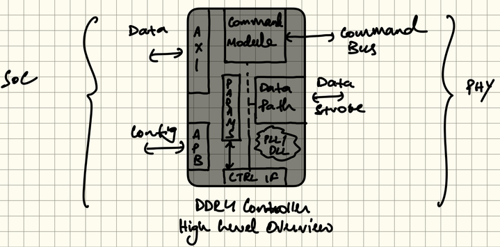
Command Module
Srimanth Tenneti is working on the definition of the Command Module and the interactions with other blocks within the DDR Controller IP.
The Command Module is responsible for forming the standardised DDR commands the the DDR Controller IP uses to drive the off chip DRAM devices.
The JEDEC standard describes a set of DDR commands. These commands are defined by state of the signals of the physical layer ("PHY") interconnect (CS_n, ACT_n, RAS_n/A16, CAS_n/A15, WE_n/A14 and CKE) at the rising edge of the clock.
Command and Address lines are uni-directional signals from the memory controller to the DRAM devices. The clock signal ("CLK") is critical for synchronization and operation of the memory system.
-
Timing Parameters Module
Dhanaji Pawar was to work on the Timing Parameters Module.
The external DRAM memory devices require time to fully execute DDR commands. As DRAM memory devices can come from different manufacturers and can be connected via different physical interconnects, the JEDEC specification allows for programmable timing parameters. Initial timing parameters are established as part of the SoC boot sequence. This will be undertaken as part of configuring the DDR Controller which is directed by the system over the APB interface. The timing parameters are established in Timing Parameter Registers within the Timing Parameters Module. These registers and their contents are then accessed by other parts of the DDR Controller IP.
-
Data Path
The Data Path is the physical implementation of the DDR memory bus that is used to transmit data between the on-chip memory controller and the external DRAM memory devices. The data path is bidirectional, during write operations data needs to pass from the controller to the DRAM and during read operations data needs to pass from DRAM to the controller, synchronised on edges of the clock signal.
As well as the signal paths for the transmitted data ("DQ") there are data strobe ("DQS") and data mask ("DQM") signals. When high DQM signals suppression of data transmission, data should not be read or written. DQS is used to synchronize the sampling of the DQ and DM signals. For a write operation the controller is responsible for establishing the data signals halfway between two DQS transitions. On read operations the DRAM device will establish the data signal in line with with DQS. It is the controllers responsibility to delay data and/or strobe signals in order to latch the data successfully using the DQS. Timing must accommodate for delays caused by the physical interconnect.
Team


 Srimanth Tenneti
Researcher
at University of Cincinnati
Research area: Machine Learning | SoC Design
Submitted on
Comments
Background materials for the project
Hi Shrimanth, can you please mention some resources for reading which could help prepare with the pre-requisites to work on the project?
LPDDR Based Memory Architecture
Hi Folk,
You can check out this website to get some insights into the LPDDR Memory Architecture. The exact spec is not yet finalized yet and will let you know the details once I have it (ETA : 1 Week).
Thanks, & Regards
Srimanth Tenneti
Link: https://www.systemverilog.io/design/lpddr5-tutorial-physical-structure/
Introduction
Hello Everyone,
We are planning to organize a meeting sometime next week to kickoff the project and introduce ourselves. Could each one of you post your areas of interest (related to the project) for us to get an understanding of the team we have here ?
Also kindly let us know your availability (Time and Time Zone) for a meeting on Friday next week.
Thanks & Regards
-Srimanth Tenneti
Template :
Name :
Areas of Interest : Micro-Architecture/RTL Design/STA/Physical Design/Verification/ ...
Srimanth Tenneti - Areas of Interest
Name: Srimanth Tenneti
Areas of Interest: Micro-Architecture, RTL Design (Verilog / System Verilog), Static Timing Analysis, & Physical Design
Hi, My areas of Interest are…
Hi,
My areas of Interest are STA and Physical Design. My time zone is Indian Standard Time (GMT + 5:30), and I am fine any time outside work hours (10:00 to 17:00).
Hi, My areas of Interest are
Name: Dhanaji Pawar
Areas of Interest : Micro-Architecture/RTL Design
Area of interest - Sandeepan Roy
Name: Sandeepan Roy
Area of Interest: RTL Design(Verilog, System Verilog), Microarchitecture, Simulation based Verification (Universal Verification Methodology)
Availability on Friday: 18:00 - 23:00 hours (GMT +5:30, Indian Standard Time)
Hi everyone,Name: Vaishnavi…
Hi everyone,
Name: Vaishnavi Joshi
Area of Interest: Micro-architecture, RTL Design, Machine Learning
My time zone is EST, and I am available on Friday evening from 6pm onwards
Meeting times
Hi,
We are holding the meetings on Friday at 3pm UK time. We are wondering if there was a better time? Have you been able to keep up with the project either here or on the slack channel?
We look forward to hearing from you.
GitLab acount
Hi,
I have created my GitLab account with username "Sandeepan26'. Pleas add me to the Soc Labs group.
Added you to the project
Added you to the project
Intro and areas of interest
Hello everyone,
I am Sarika, a grad student, interested in hardware design, specially in RTL design and Physical Design. I am very excited to learn from the team and contribute towards this project.
Thank you.
DDR4 SDRAM specification
Hi,
I am here to ask if the JEDEC specification for DDR4 SDRAM is accessible to any member in this group. Based on my understanding of DDR4 SDRAM, the design is based on DDR Controller and DDR PHY. If the specification could be accessed, then the design could be learnt in-depth.
Here is the link for DDR4 specification: https://www.jedec.org/standards-documents/docs/jesd79-4a
Interested in Collaboration for the project
Hi
My self I have Naveen
Area of interest:Verification , RTL Desgin ,Physical desgin .
Skills:verilog,system verilog ,UVM,Python
Verification Methodology
One of the tasks within the Architectural design flow is the definition of the verification methodology. This is an interesting paper of a Framework for Formal Verification of DRAM Controllers.
Perhaps we should dedicate one of our meetings to looking at verification.
Some additional papers
Work by Kirill Bykov on acceleration of the RTL simulation of any memory controller.
Project needs a more detailed description
I think the project needs an updated description. There is a nice level of detail in this project:
GitHub - AngeloJacobo/UberDDR3: Opensource DDR3 Controller
John.
UberDDR3
Angelo has made the point that if the controller is for AI/ML applications, then the controller needs to be fast. He believes UberDDR3 is fast compared to commercial DDR3 controllers like the Memory Interface Generator (MIG) in Vivado, but uses much less area than the MIG.
His recent blogpost discusses a Dhrystone Test comparing the performance of MicroBlaze with UberDDR3 against MicroBlaze with MIG.
Dhrystone test performance results:
MicroBlaze with UberDDR3 = 0.3154 DMIPS/MHz
MicroBlaze with MIG = 0.3061 DMIPS/MHz
UberDDR3 uses 32.63% fewer Slice LUTs and 32.33% fewer Slice Registers than MIG.
The PHY used by UberDDR3 is specific to Xilinx 7-series FPGA.
Code reading and Comments
I must draw the attention of the team to the quality of comments Angelo has put in the UberDDR3 project. It is an example to all to follow.
Add new comment
To post a comment on this article, please log in to your account. New users can create an account.