




People






University of Southampton
|
Country
United Kingdom of Great Britain and Northern Ireland (the)
| |
 Members
 |
48 |
 Projects
 |
40 |
 Articles
 |
8 |
 Contributor since:
 |
Wed, 06/30/2021 - 14:50 |
| AAA Member |
Actions
Projects
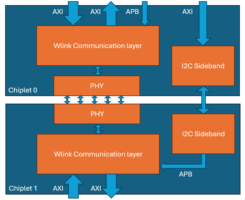
For a chiplet system, you need a communication interface between chiplets. The industry has developed standards that require complicated IPs around UCIe and the CHI interface from Arm. For many academic projects these are probably more complicated than needed . The aim of this project is to produce a simple chiplet communications interface based around the open standard AXI protocol.
The project is hosted here: https://git.soton.ac.uk/soclabs/chiplets/axi-chiplet-controller
 Daniel Newbrook

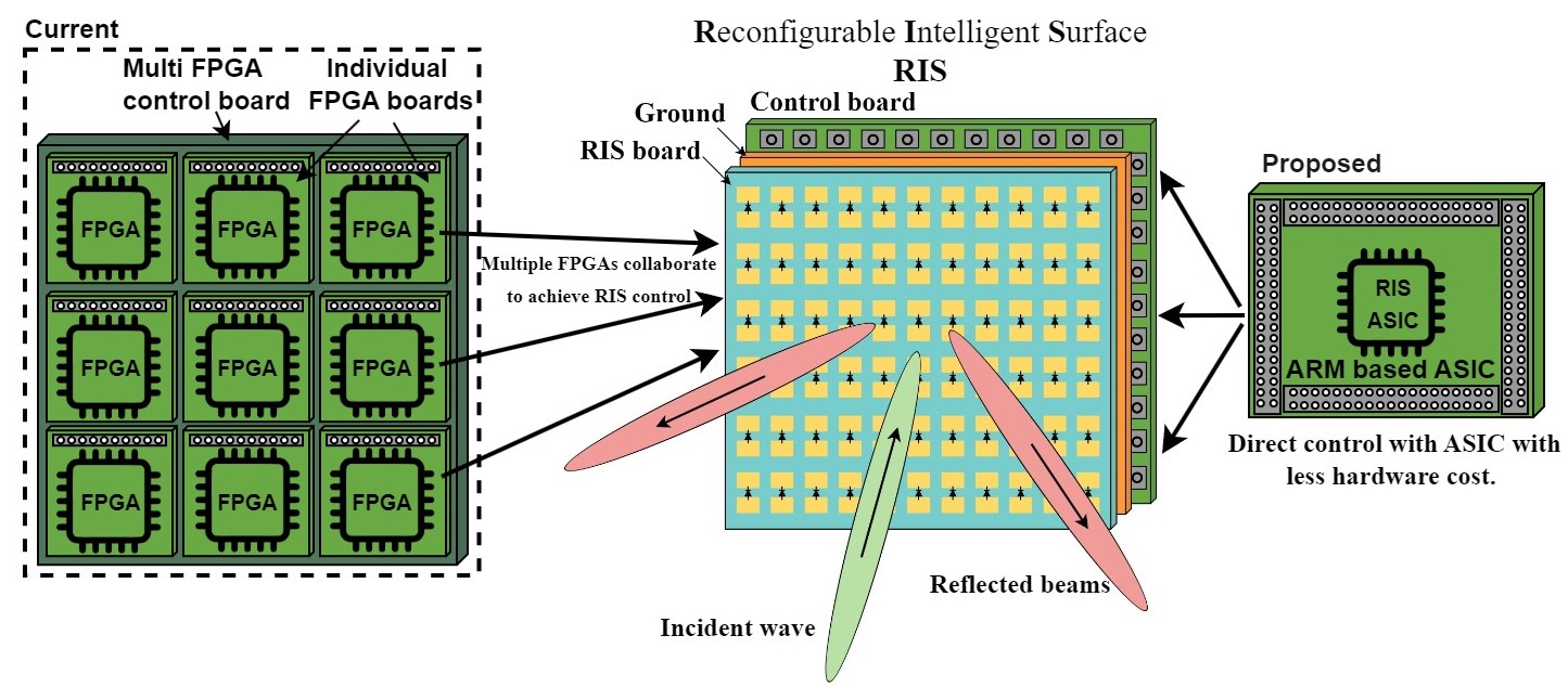
Reconfigurable Intelligent Surfaces (RIS) are planar structures composed of large arrays of tunable elements that can dynamically redirect, reflect, or shape wireless signals in the environment.
 Zhicheng Shen
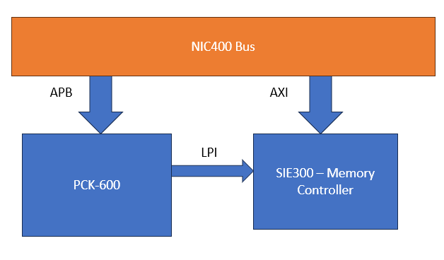
The PCK600 Arm IP provides components to allow a power control infrastructure to be distributed in a SoC in order to make a design energy efficient. Arm provide the IP as part of their Power Control System Architecture that can be used to control the power states of various parts of the system. This control of the power infrastructure is achieved through the use of the Power Policy Unit (PPU). This unit has an APB interface to allow for software control, and some low power interfaces that can connect to the power controllable IP within the system.


This program is dedicated to the development of a System on Chip (SoC) platform, specifically designed to support learning and research activities within Indonesian academic institutions. The platform serves as an educational and research tool for students, lecturers, and researchers to gain hands-on experience in digital chip design.

 Trio Adiono