Use the Tabs below to find information on community projects. Project pages have links to the 'technology' and 'design flow' stages used and ways you can comment on or join a project.
- Projects are key to community hardware design
-
As a community hardware design activity we form our collaborations around shared design actions making Projects a core of the SoC Labs community. Projects help us share and reuse hardware and software developments around core Arm IP to help us in our research goals.
- A project, takes technology and uses a design flow to make a SoC.
-
A project has a timeframe and uses the two other significant aspects of a SoC development, the selection of technology or IP blocks that make up the SoC and the design flow that is followed from specification through to final instantiation of a system. Any System On Chip usually involves the use of pre-existing IP blocks. A project team can select IP from the technology section of the site during the first stage of a design flow, Architectural Design. Later stages in the design flow support the creation of the novel aspects of the SoC design.
- Projects have a type, either active, complete (case study) or being formulated (request for collaboration)
-
Sharing information on projects much earlier than traditional academic collaboration is encouraged. Historically knowledge sharing has been at the end of the research activity, with published papers and results. As well as write up of finished projects ("case study"), ongoing projects under development ("projects") there are projects that are still being formulated ("request for collaboration") listed. We want to encourage people to engage with the project teams, for example, adding a comment to a specific project page or joining a project.
Latest Reference Design Projects
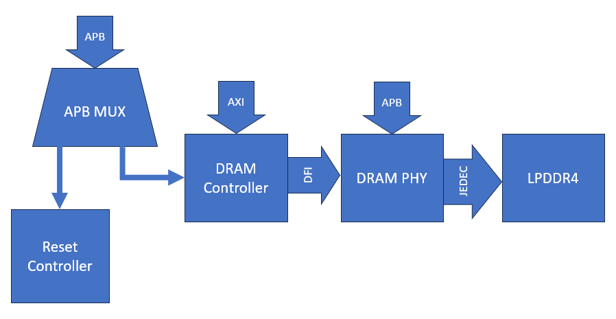
To enable full operating system support in megaSoC, a substantial amount of memory is required to accommodate the complexity of modern Linux-based software stacks, including the kernel, drivers, middleware, and user-space applications. Linux environments, unlike lightweight bare-metal systems such as nanoSoC, demand not only larger memory footprints but also consistent access to high-bandwidth memory to maintain performance across multitasking workloads. The most common approach is to incorporate external DRAM, which offers the necessary capacity and throughput.

 Daniel Newbrook
 David Mapstone
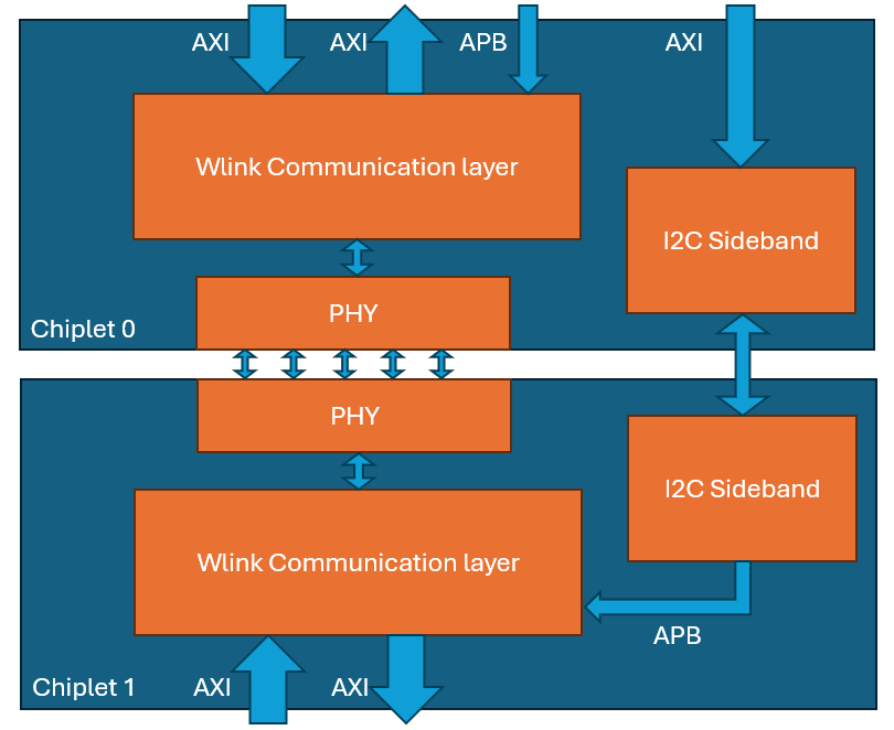
For a chiplet system, you need a communication interface between chiplets. The industry has developed standards that require complicated IPs around UCIe and the CHI interface from Arm. For many academic projects these are probably more complicated than needed . The aim of this project is to produce a simple chiplet communications interface based around the open standard AXI protocol.
The project is hosted here: https://git.soton.ac.uk/soclabs/chiplets/axi-chiplet-controller
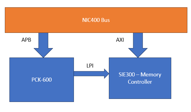
The PCK600 Arm IP provides components to allow a power control infrastructure to be distributed in a SoC in order to make a design energy efficient. Arm provide the IP as part of their Power Control System Architecture that can be used to control the power states of various parts of the system. This control of the power infrastructure is achieved through the use of the Power Policy Unit (PPU). This unit has an APB interface to allow for software control, and some low power interfaces that can connect to the power controllable IP within the system.
Latest Collaborative Projects
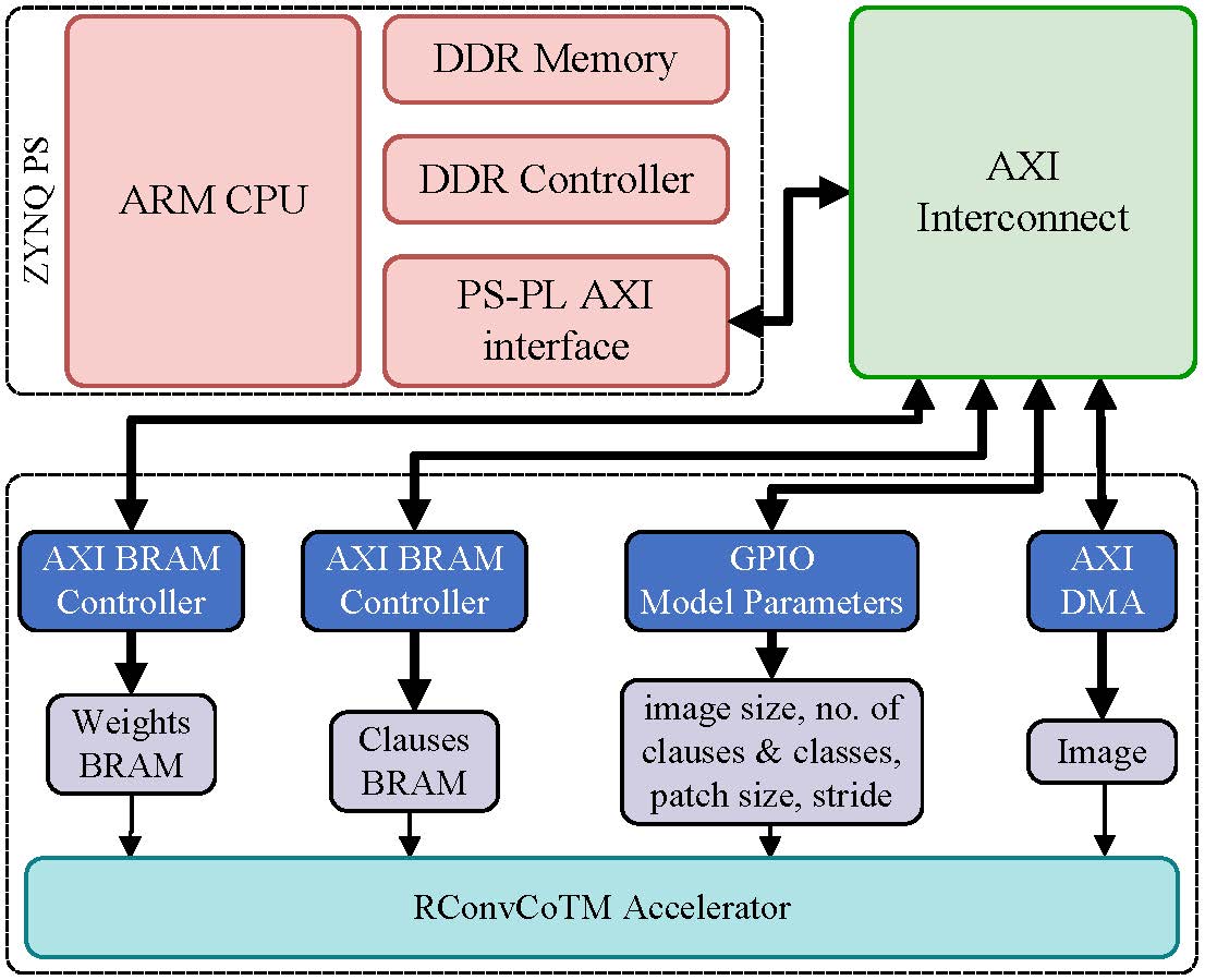
In this project, we would like to integrate our TsetlinMachine Hardware Accelerator into nanoSOC and tapeout the design.

 Srinivas Boppu
 Shiva Sangati
Precision timekeeping is a foundational service in any distributed system. Whether synchronising Ethernet frames to a PTP grandmaster, timestamping die-to-die packet exchanges between chiplets, or scheduling time-critical hardware events, the system needs a clock that is accurate, capturable at multiple points simultaneously, and adjustable by both hardware servo loops and software without stopping.
Latest Competition Projects
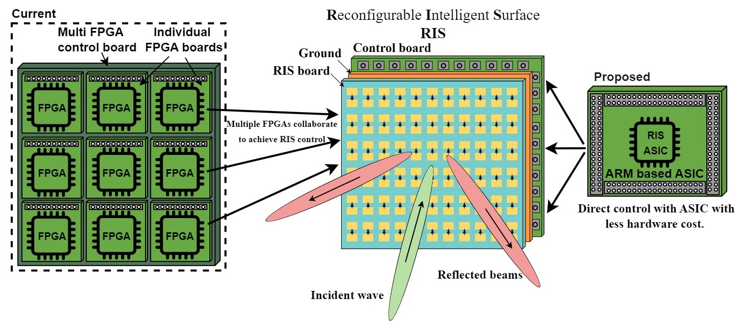
Reconfigurable Intelligent Surfaces (RIS) are planar structures composed of large arrays of tunable elements that can dynamically redirect, reflect, or shape wireless signals in the environment.
 Zhicheng Shen
This project aims to develop an advanced RF energy harvesting (EH) receiver chip specifically designed to power embedded sensors for monitoring the condition of groceries during transportation. The receiver chip captures wireless energy transmitted from phased array antennas and converts it into electrical power that is used to operate onboard sensors, which continuously monitor critical parameters such as temperature and humidity inside delivery trucks.

 Fidel Makatia
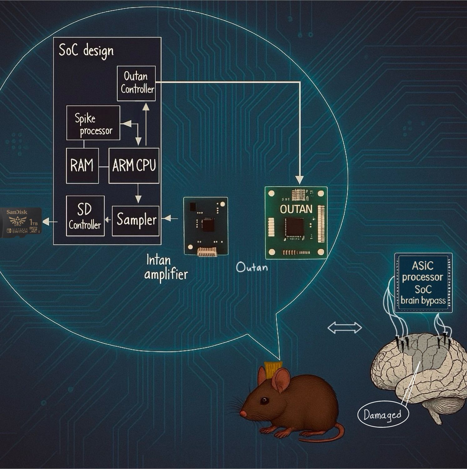
Stroke and epilepsy are among the most common debilitating neurological conditions, with a worldwide prevalence of 100 million people (World Stroke Organization, 2022) and 50 million people (World Health Organization, 2024), respectively. Present-day approaches for treating neurological and neurosurgical conditions include physiotherapy, pharmacological treatment, surgical excision, and interventions such as deep brain stimulation.
In the context of Industry 4.0, handwritten digit recognition plays a vital role in numerous applications such as smart banking systems and postal code detection. One of the most effective approaches to tackle this problem is through the use of machine learning and neural network models, which have demonstrated impressive accuracy and adaptability in visual pattern recognition tasks.

 The Anh Nguyen
Latest Completed Project Milestones
| Project | Name | Target Date | Completed Date | Description |
|---|---|---|---|---|
| SDIO Controller Verification | Getting Started |
Project scope: Integration of the ZIP CPU SDIO Controller as a submodule of MegaSoC project. |
||
| SDIO Controller Verification | Synthesis |
|
||
| SDIO Controller Verification | RTL Verification |
|
||
| SDIO Controller Verification | Simulation | |||
| DRAM Controller integration in megaSoC | IP Selection | |||
| DRAM Controller integration in megaSoC | Specifying a SoC | |||
| DRAM Controller integration in megaSoC | Verification Methodology | |||
| DRAM Controller integration in megaSoC | Architectural Design | |||
| DRAM Controller integration in megaSoC | Getting Started | |||
| DRAM Controller integration in megaSoC | Generate RTL |