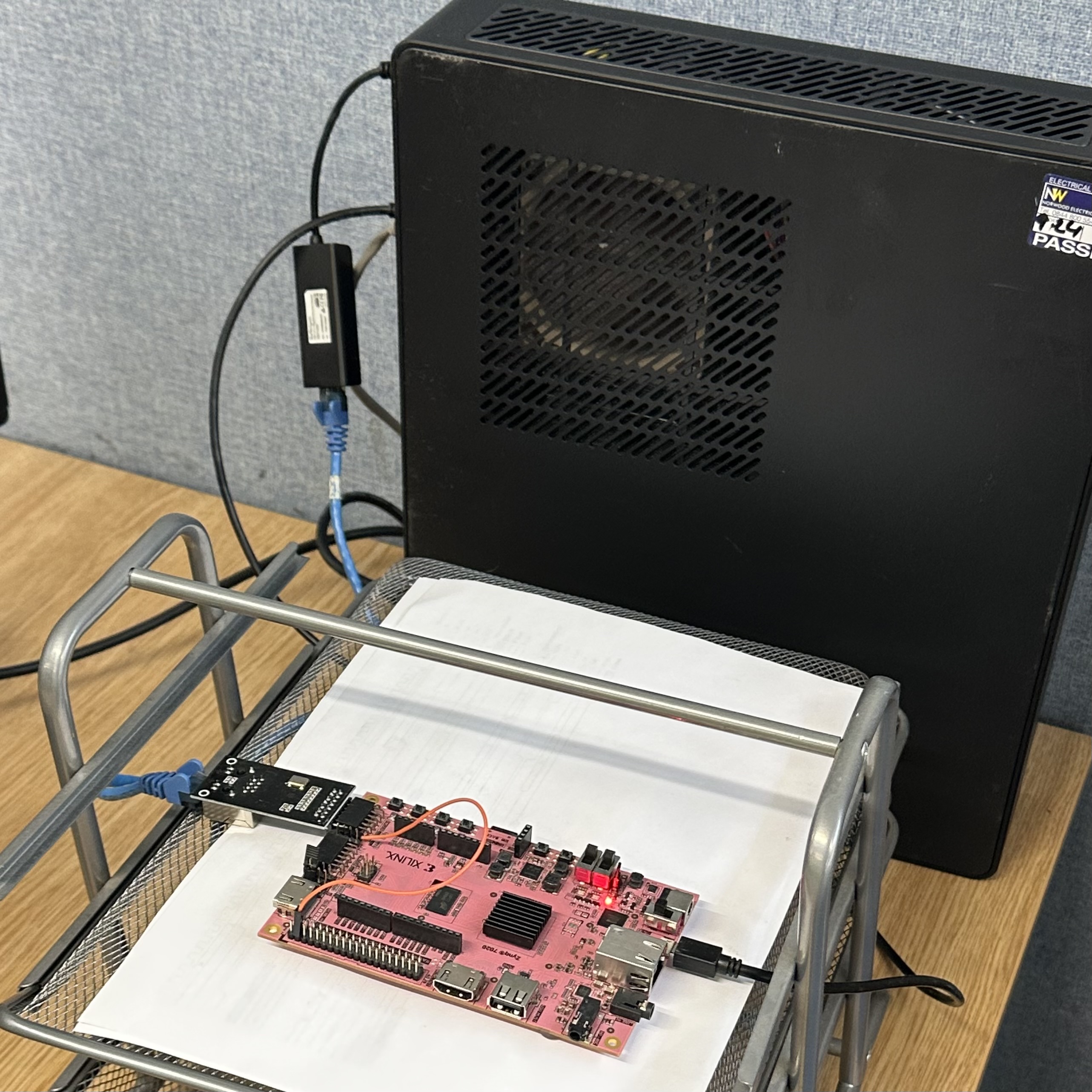
View Collaborative Projects


This program is dedicated to the development of a System on Chip (SoC) platform, specifically designed to support learning and research activities within Indonesian academic institutions. The platform serves as an educational and research tool for students, lecturers, and researchers to gain hands-on experience in digital chip design.
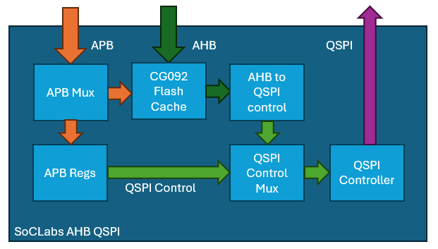
The instruction memory in the first tape out of nanosoc was implemented using SRAM. The benefit was the read bandwidth from this memory was very fast, the downside was on a power-on-reset, all the code was erased as SRAM is volatile memory. An alternative use of non-volatile memory would benefit applications where deployment of the ASIC does not allow, or simply time is not available for programming the SRAM after every power up.
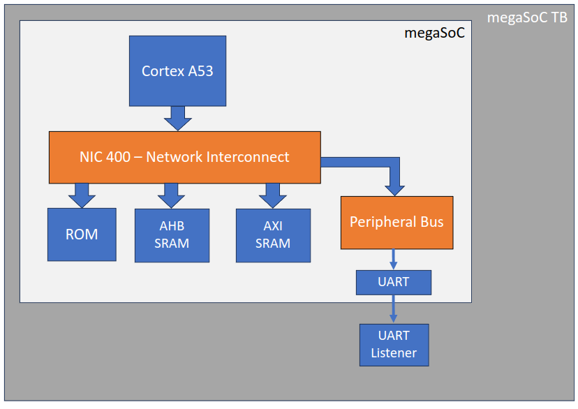
There is growing interest within the SoC Labs community for an Arm A-Class SoC that can support a full operating system, undertake more complex compute tasks and enable more complicated software directed research. The Cortex-A53 is Arm's most widely deployed 64-bit Armv8-A processor and can provide these capabilities with power efficiency.
This project aims to design and implement a high capacity memory subsystem for Arm A series processor based SoC designs. The current focus of the project is the design and implementation of a Memory Controller for DDR4 memory.
The Synopsys HAPS® System adds additional capabilities to the FPGA-based prototyping environments SoC Labs can use to support projects. The HAPS® system provides a greater amount of logic resources supporting development of larger SoC designs. It can be used to support multiple projects simultaneously. It is used by many semiconductor companies, including arm for their CPU verification. This collaboration project will use the HAPS® system in SoC Labs projects and share with the community experience in utilising such systems.

This collaboration project is aimed at providing specific tailored activities to the local geography in Canada by developing local actions that will help stimulate academics and their institutions and the broader semiconductor industry supporters to create new and exciting SoC design projects. It may include:

The Arm PL022 provides an interface for synchronous serial communication with peripheral devices connected to the SoC via the Advanced Peripheral Bus (APB). It supports a choice of interface operation, Motorola compatible Serial Peripheral Interface (SPI), National Semiconductor Microwire, or Texas Instruments synchronous serial interface. See the Techology page for details.

To design and verify a simple PLL for use as generator of clock signals in System on Chip design. The desired outcome from this project should be the following:
Clock generation for frequencies between 60 MHz and 1.2 GHzInclude PLL-lock signal for system start upLow clock uncertainty below 5% (transition time and jitter)Integer clock divider which can be updated at run timeMinimal areaThe resulting IP for these component blocks will be made available to the soclabs community for the upcoming design contest.
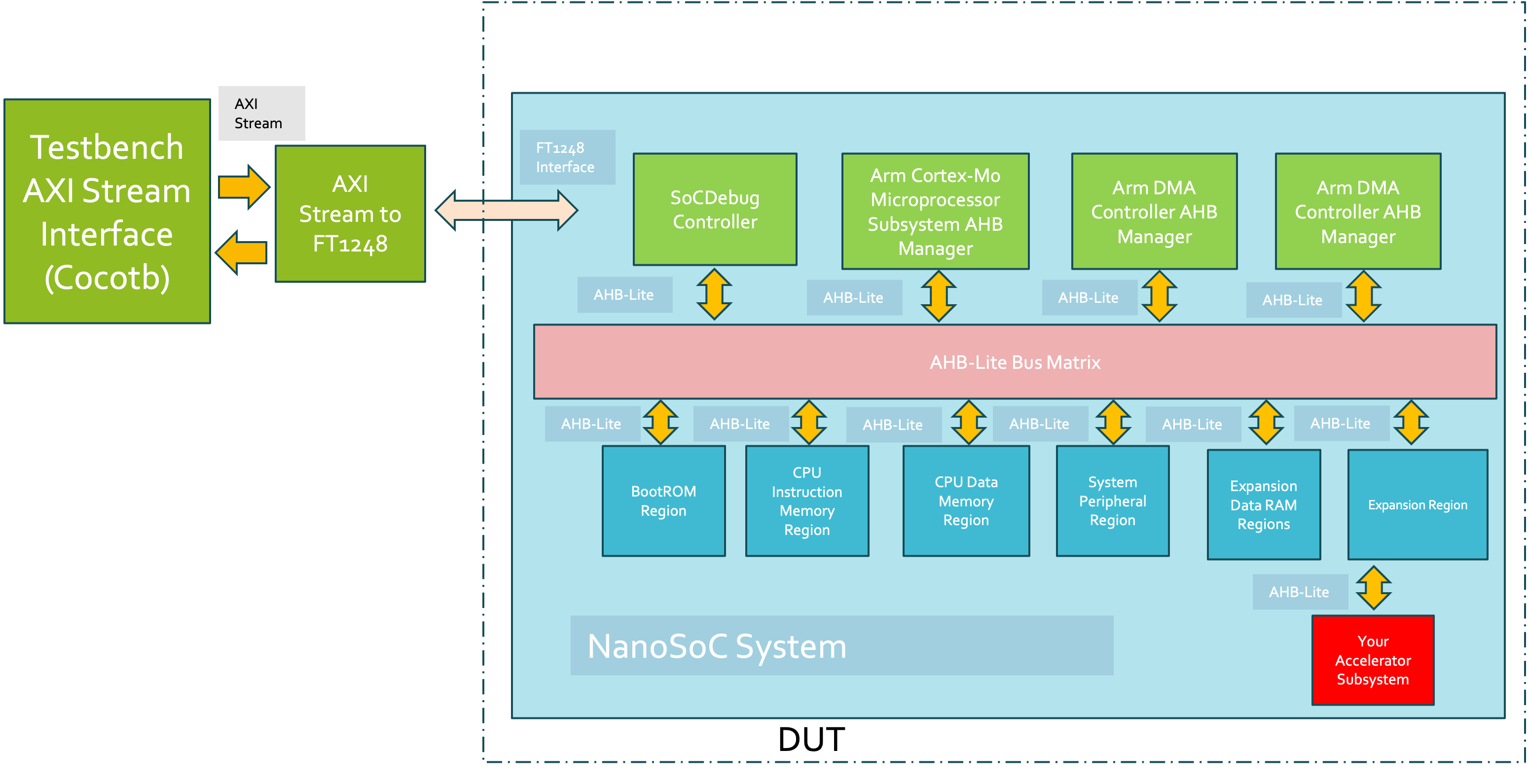
Performing system-level verification on a System-on-Chip (SoC) design is crucial for ensuring the correct function and overall performance of the entire system, rather than individual components. This project is aimed at developing the necessary resources and design flow stages for the verification of the NanoSoC reference design.
Architectural Design: Verification MethodologyWith NanoSoC, there are multiple options for performing system-level verification.

 David Mapstone
 Trio Adiono
 Daniel Newbrook

 Srimanth Tenneti


 John Darlington
