






Architectural Design
Introduction
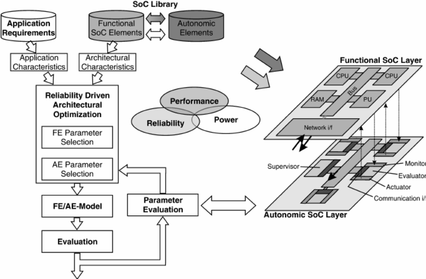
The concept of reusable design patterns is familiar to many disciplines. At SoC Labs we are interested in reusable design patterns incorporating Arm based components to form the core of the System on Chip ("SoC") with parts added that are unique to your specific research challenge.
Arm itself uses the term Architecture for defining the processor instruction set, programmers' model and memory model, but not the implementation details such as cache sizes, data transfer widths, etc. Your SoC design is likely to be a selection and configuration of Arm IP to define the main architecture for the overall system. Arm provide Corstone Subsystems that combine the various system IP components for a specific processor and Arm architecture to simplify System on Chip design. It is most likely a SoC Labs project will use one of these subsystems adding specific blocks either developed uniquely or existing third party blocks modified or arranged in a novel way.
SoC Labs is enhancing the baseline Corstone subsystems to make them more easily adopted for academic needs and projects.
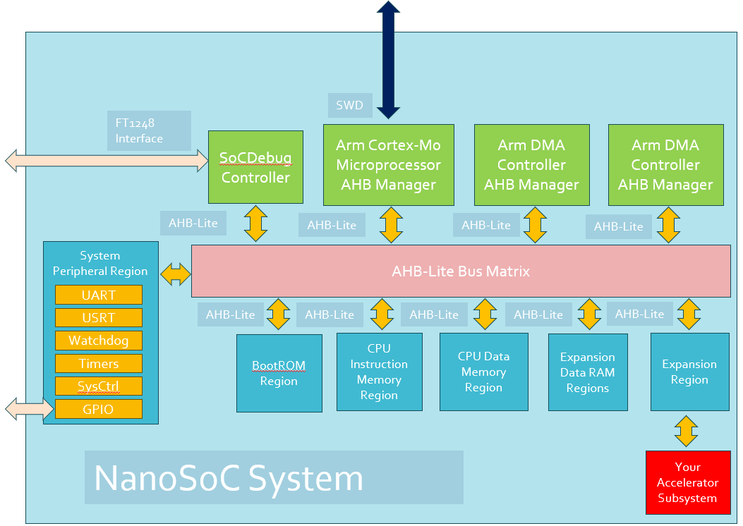
nanoSoC extends the Corstone 101 subsystem
milliSoC extends the Corstone 300 subsystem
megaSoC extends the Corstone 1000 subsystem
Getting Started
The first step is describe in a Specification for the SoC a list of the proposed uses, specific algorithms or calculations that are to be implemented, what are the data requirements, time critical operations, etc. These help decide which compute subsystem / reusable reference designs is best.
At this high level stage of the design process project budget, available time and manpower may be constraints on what is achievable as well as project goals on ultimate energy efficiency, area cost or system performance characteristics.
In making architectural design choices there are some tools available. These usually rely on pre-determined static information for area, power and performance that are adjusted/calculated from any configuration specified. These can aid high level selections such as which processor to use or support more fine grained choices in terms of data paths, cache sizes, etc.
Separation of Concerns
One technique for controlling the complexity of SoC design is to use the system Architecture to separate aspects of the design task into specific parts of the system by defining unique sub-systems or using re-usable blocks.
Some projects in SoCLabs are purely digital and some have analog interactions with the physical world. In the Arm system architecture slower speed sub-systems such as interfaces to the external environment are usually placed on a separate Advanced Peripheral Bus to ensure the core high speed functions of the systems such as the CPU to memory interface can operate efficiently. An example of this is the project to define a mixed signal subsystem for the nanosoc reference design. Sub-systems such as custom compute accelerators for Machine Learning and Artificial Intelligence need high through put of data and need to be on the main system bus. For nanoSoC there is an example of how a custom accelerator is integrated within a SoC
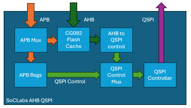
The ARM Advanced Microcontroller Bus Architecture is an open-standard, royalty-free, platform-independent, architecture for the connection and management of functional blocks in System On Chip design. SoC Labs projects will most likely integrate components into this bus architecture.
Another separation of concern is the design of the hardware and the implementation of the software system although they are inter-related. For example when considering a specific algorithm it is worth considering the relative performance of using one of the Arm processors running software versus developing a hardware custom accelerator. Estimates of instruction and data bandwidth will be needed in order to determine what memory is needed for intermediate storage. This is especially true when it comes to Machine Learning / Artificial Intelligence workloads.
Data Movement Considerations
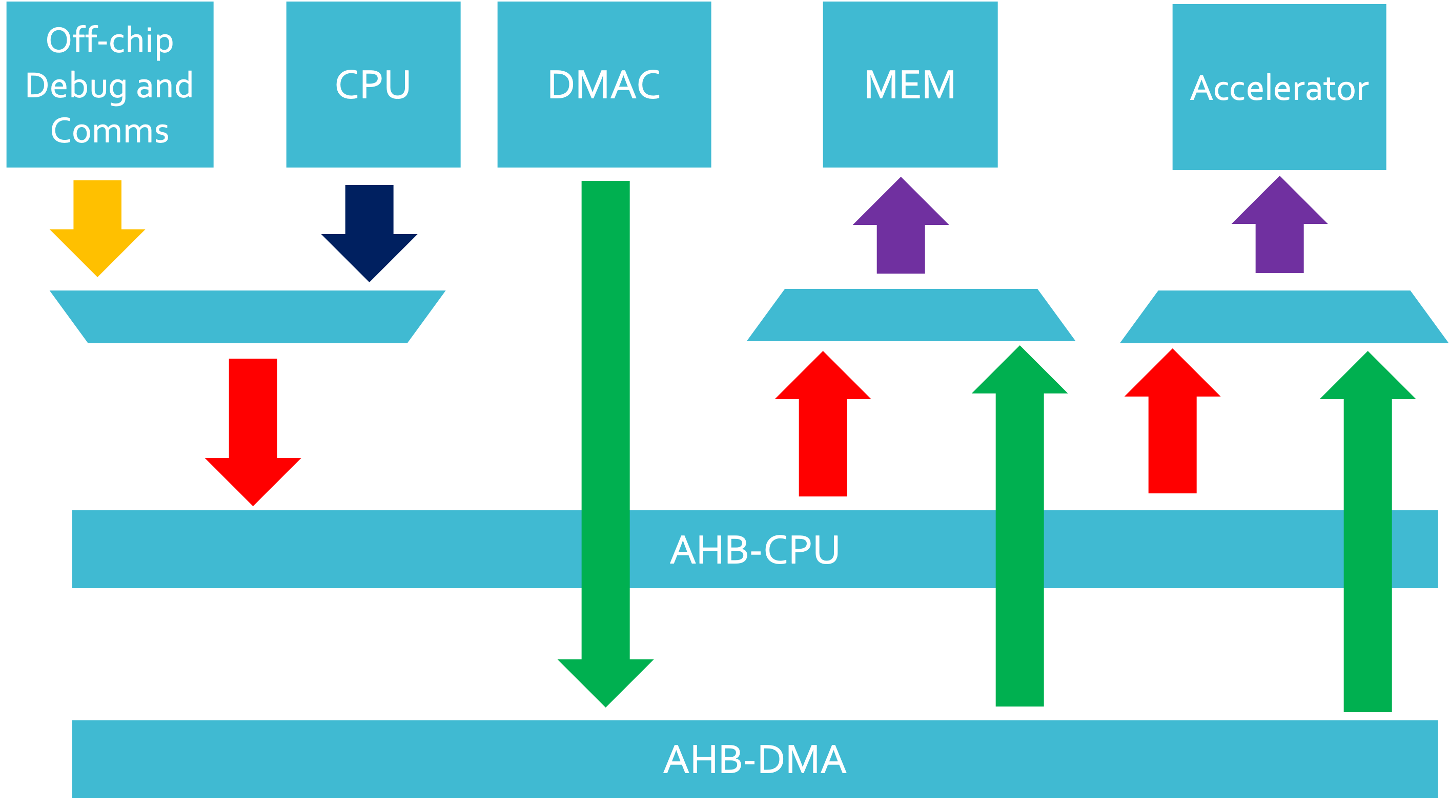
A proposed Architecture needs to specifically consider the flow of data within the system as a whole. It needs to consider how data will be moved to/from the external environment into the system and through any processing and storage stages. As well as primary data flows for the core operations of the system, secondary data flows such as debug information for error conditions and any systems start up specific flows, etc. need to be considered. Much of the detailed choices have already been considered in the various corstone subsystems and SoC Labs reference designs that extend them for academic projects. The SoC Labs Reference Design Comparison Table provides some high level comparisons of the data movement options.
The overall system data flow between the various components, subsystems and the external environment are needed to determine the bus systems to interconnect them. In more complex systems, a network-on-chip (NoC) architectural design as implemented in the corstone 300 and 1000 may be justified. There is a basic project here on building system-optimised AMBA interconnect.
Within a subsystem local exchanges via hardwired data paths are more efficient than switched structures such as buses and NoCs and keeping wiring lengths short allows energy use to be minimised.
Memory Considerations
Memory requirements place significant constraints on a proposed Architecture. Memory is usually laid out using specific technology node memory compilers. Placement of these blocks within the system can have implications on routing of interconnect between components.
System Throughput Considerations
It is important to consider any time critical operations of the system and cycle times for any system operations. This will allow a determination of the target clock frequency for the SoC as well as the degree of any parallelism in operations that can be implemented. This approximate target clock frequency may differ from the final solution but having an initial target will help determine the likely power consumption and outline costs of an ASIC implementation.
Architectural Design System Decomposition / Partitioning
Given an initial Specification of the needs of the system an outline system architecture for the project can be made. Hopefully this fits one of the profiles for the SoC Labs reusable reference designs which should drastically simplify the selection of design components. Once all the reusable IP parts have been selected the custom developments and parts that are unique to the specific research challenge can be outlined and the task of considering the interfaces between the system's components, subsystems, and the external environment. If one of the SoC Labs reusable reference designs is not appropriate it may be possible to use tools to automate much of the configuration of the interfaces and interconnect for an more novel System on Chip design. Arm provide the Socrates Interconnect Tool to configure IP components using an AMBA® interconnect that can be tailored to the specific project goals.
These tools may only be able to guide the initial partitioning for typical SoC projects as there is a large design space of decisions for any particular design in order to optimise various system characteristics including energy, area, execution perform, etc. The design may evolve in a process of architectural exploration where different configurations of IP blocks are considered and relative benefits evaluated.
Subsytem Design Decomposition
Once the main system architecture has been outlined the specific sub-systems within it can be decomposed.
Explore This Design Flow


Projects Using This Design Flow




Experts and Interested People
Members



Related Project Milestones
| Project | Name | Target Date | Completed Date | Description |
|---|---|---|---|---|
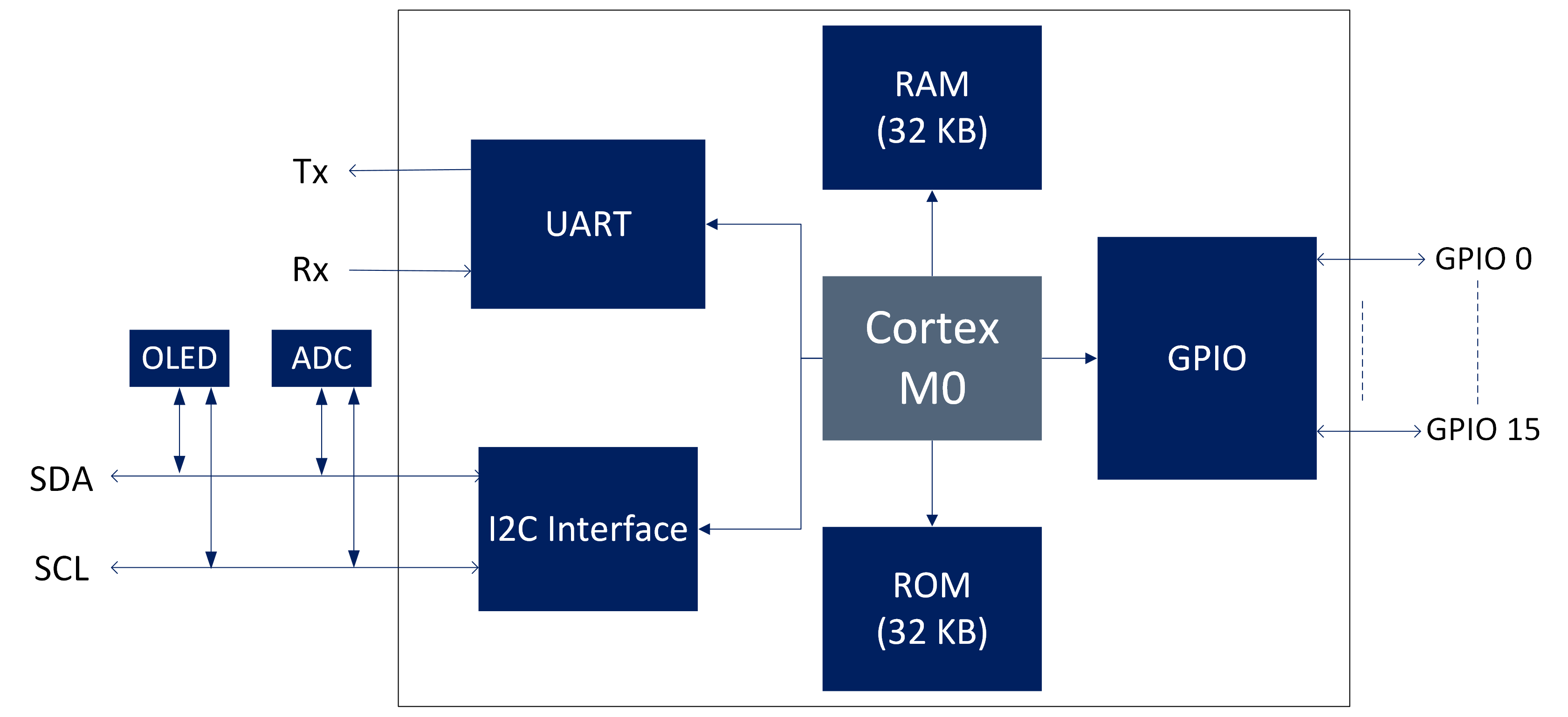
| ARM Cortex M0 Based SoC for Biomedical Applications | Architectural Design |
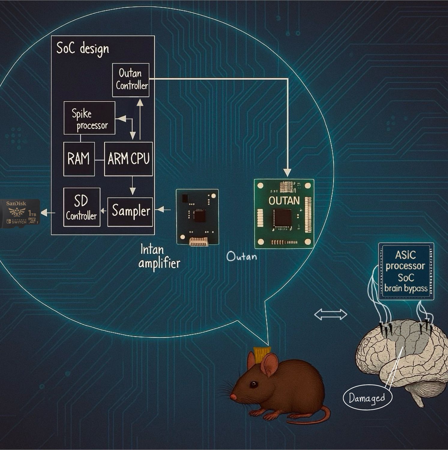
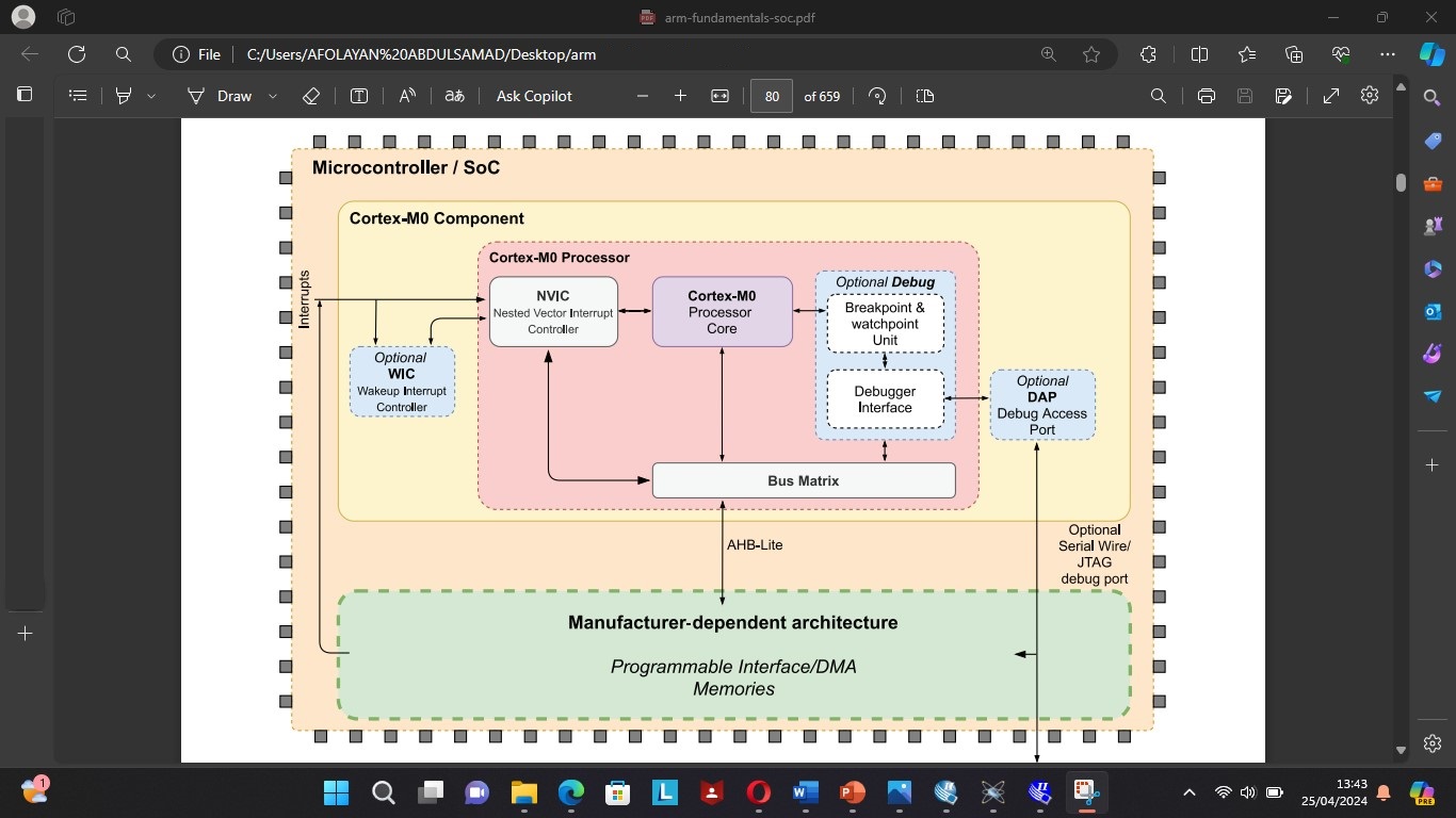
In this milestone, we aim to define the hardware used in the SoC. Behavioural level code has been written in Verilog to allow protocol conversion between AHB Lite protocol used in ARM Cortex M0 and UART/I2C peripheral. |
||
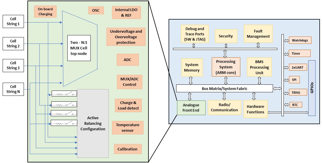
| Battery Management System-on-chip (BMSoC) for large scale battery energy storage | Architectural Design |
|
||
| Interference Detection and Mitigation Accelerator for Automotive Radar SoCs | Architectural Design (92) |
Architectural Design of Accelerator Modules
|
||
| Low-Cost and Low-Power Data Acquisition System(DAQs) for Real-time Data Collection | Architectural Design |
Requirements Specification: The DAQs has two modules - the Gateway and the End-terminal. End-Terminal Requirements: Purpose: Outdoor device for gathering real-time environment data Inputs Power button, 5 sensor connectors: Outputs: Antenna, 3 indicators - active, low power & power good Functions: monitors 5 water quality parameters - PH, TDS, Temperature, Turbidity & ???; transmits |
||
| IMPLEMENTATION OF FIXED TIME BASED TRAFFIC LIGTH SYSTEM USING FPGA WITH VERILOG HDL. | Architectural Design |
structural design of the project |
Comments
Expanding upon Architectural Considerations
There are a number of considerations that need to be made at the architectural design phase which really impacts the design decisions later on. With hardware design, it always comes back to PPA - Power, Performance and Area. Having a performant architecture will usually have adverse implications on the power and area of the design in both FPGA and on ASIC. This means whenever a SoC architect is designing a new system, they will need to consider the trade-offs and work out the point that satisfied all criteria.
For research projects, all three are very important, area especially for budgetary constraints. Have large numbers of SRAMs on chip for example, while they may improve performance and allow for better buffering techniques, especially in bursty applications, will have massive impacts on the area of a die. This is less important in FPGA implementations where there are usually MBs of BRAMs on chip, but for small ASIC designs, you often want to tune the size of your SRAM macros and then consider whether it is better to have multiple memories or one large one for area and performance impact.
To be able to do this, it is important to think about traffic conditions and where data is moving within your SoC. Are there direct channels between your CPU and memory for example or is it going over an arbitrated bus and what impacts does this have when other devices are trying to communicate over this bus too? How does the increased bus complexity impact the area and performance of your SoC? And how can this properly be verified and validated?
Thinking about the types of traffic moving in the system is important too and how this impacts what you're trying to achieve. Is data continuous and what are the implications of that on caching and buffering? What if the data requires higher bandwidth but is more bursty? What happens in the case of back-pressure and stalling within components in your system? Do they lock up and stop processing, are they well fed, do they have a specific amount of output buffering so they can keep processing? Understanding these behaviours of components in your system should decide how not only you shape your architecture of the SoC, but also the architecture of sensory and accelerator subsystems you might be designing.
The point here being picking up a SoC off the shelf may get you so far, but modifying and analysing the architecture of the SoC, with your specific application case is an important step before hardening.
Add new comment
To post a comment on this article, please log in to your account. New users can create an account.